In a world where AI is energy-hungry, the Tensor Processing Unit (TPU) is a game-changer. It is a custom-built chip designed by Google specifically for machine learning tasks.
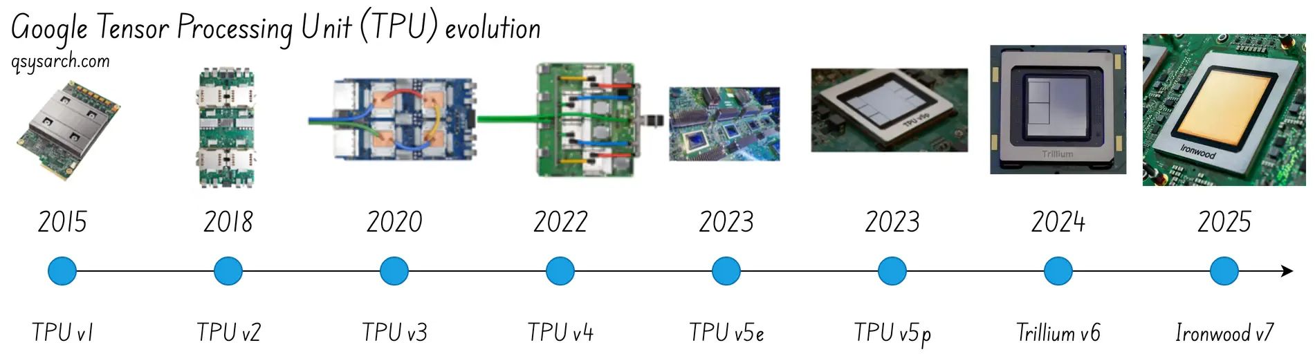
This quick memo is an attempt to provide a high-level system view of the TPUs’ architecture and how they have evolved since their inception in 2016.
I will also try to answer this essential question: why do we need TPUs if we already have GPUs? What kind of advantages do they have that the GPU does not? How do they compare to the Neuromorphic ICs? And is there any alternative architecture to the TPUs and GPUs?
 (Source: Google Cloud)
Why the TPU exists — and what problems it solves Link to heading
The TPU share the same goal as the GPU: to overcome the limitation introduced from the slowing of Moore’s Law, by enabling massive parallelism: Unlike traditional CPU which can be used to handle generic computations, and which, to some extend, has a level of parallelism via the concept of multi-core (thanks to Dennard scaling’s law), the TPU and GPU are specialized hardware designed to handle simple and specific tasks, but in a much more efficenct way that any CPU could.
At a high level, one can say that deliver much better performance and efficiency than general-purpose CPUs or GPUs by “trading off generality for performance.”

The TPU is fundamentally designed for heavy linear algebra tasks, such as matrix multiplications and tensor operations, that neural networks use.
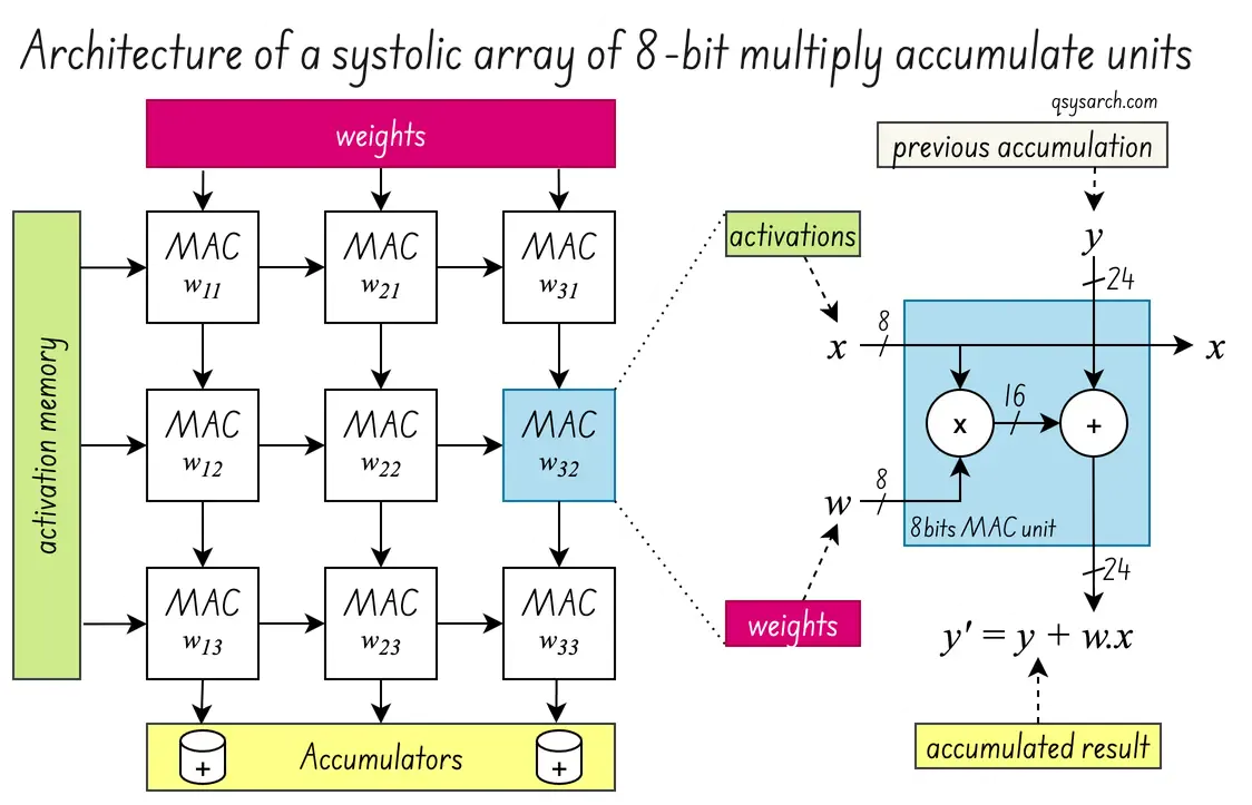
At the heart of the TPU is the systolic array, a matrix of processing elements (usually called PE, denoted as MAC on the diagram on the right) that can perform parallel computations.
In the case of the TPU, this processing unit, or MAC, is a simple 8-bit multiplier that multiplies and accumulates the activation values (the embedding) with the neural network’s weights. Only by performing this operation in a massively parallel way does the TPU achieve a much higher throughput than a CPU. And so do the GPUS! But first, let’s take a look at the evolution of TPU over time.
TPU evolution over time Link to heading
TPUv1: the first generation of TPU Link to heading
The TPUv1 was developed in just 15 months, with the principal goal of improving neural network inference (not even learning, but only inference). For this, Google needed matrix multipliers and had constraints not only on achieving high speed but also on reducing power consumption. The key to reducing power consumption was improving memory locality, e.g., reducing unnecessary data movement between external memory and TPU memory. This would allow increasing the arithmetic intensity per unit of control, i.e., reducing the TPU’s idle time waiting for data.
From the HW perspective, the TPU v1 design was straightforward yet elegantly effective:
- single threaded co-processor on a standard PCie card.
- No multi level cache, no multhreading, no branch prediction.
- Fast determinstic math on 8bits integers via the MXU, or matrix multiplication unit.
- Systolic array constist of 256 * 256 * MXU
The complexity was moved to the software scheduler, with two main responsibilities:
- keep the pipe busy, by schedule the operations in a way that the MXU was never idle.
- double buffer the memory, as a mean to hide the latency of the memory access
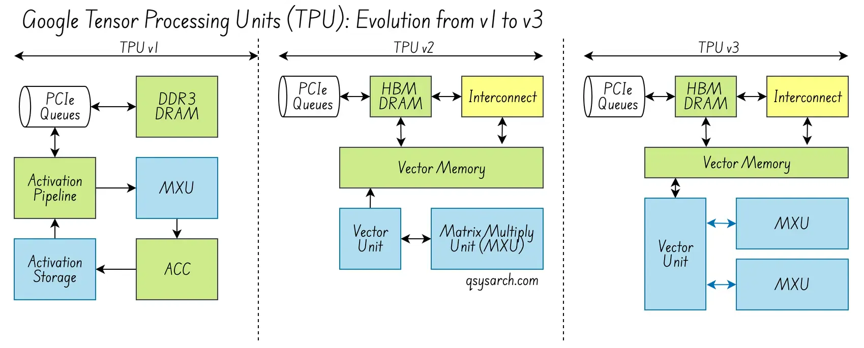
TPUv2 and v3: Improving memory and interconnect Link to heading
The key concepts in v2 and v3 are training the next generation of models that require backpropagation, higher precision, and many more distributed, interconnected TPUs.
From the HW Core Processing perspective, they introduced quite a few nice concepts:
- a dual core chip, eg one TPUv2 is made of two TPU
- Each TPU had a four time larger systolic array, consistsi of 128*128 MXU,
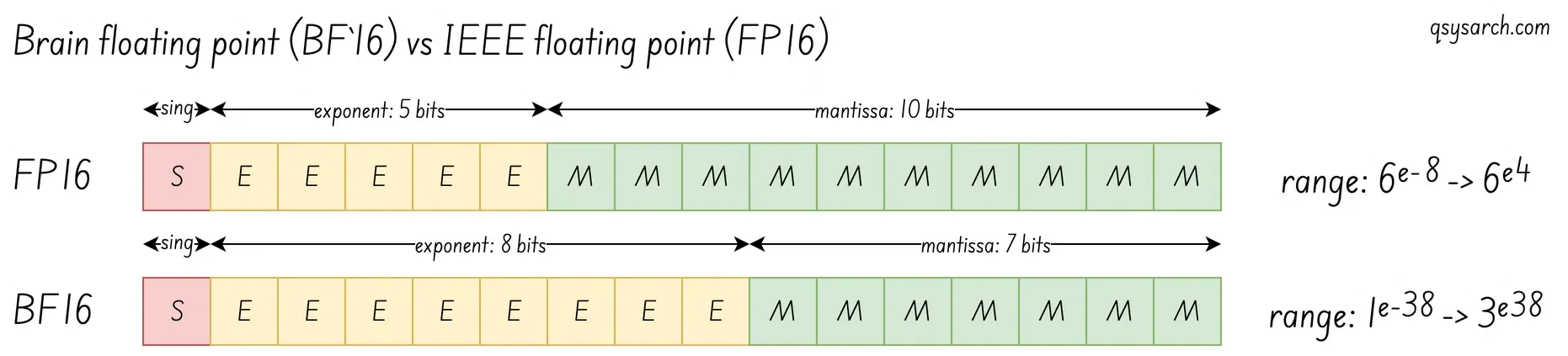
- Ability to handle floating point values, using the Brain Floating Point Format (BF16), an enhanced version of the standard IEEE 754 FP16 floating point format.
- A new high bandwidth memory (HBM) within the TPU to memory access latency; (TPUv1 only has a basic DRAM, with slow access time, while the HBM is much faster)
From the HW Connectivity perspective,
- An Inter-core interconnect (ICI), the high bandwidth fabric that allows scale, via a 16x16 2D torus network (ring network) - Super computer pod of 256 chips.
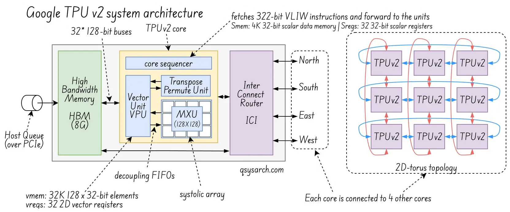
From the SW perspective, a powerful compiler:
- XLA compiler: the brain generating the VLIW instructions used by the core sequencer (TCS).
TPUv4: Hyper scale AI Link to heading
The key concept in v4 was the ability to run AI models at hyper-scale. This meant that the key driving metric was the Total Cost of Ownership (TCO).
The newest generations are designed for large-scale training. Chips are connected in racks or pods, with advanced memory systems and interconnects. They support large tensor operations, distributed training, synchronisation, and efficient data sharing across many chips.
From the HW Core Processing perspective, they introduced quite a few nice concepts:
- Spares core: prevent “zero-ops” from hitting the MXU -> improve memory utilisation.
- Memory Cache: (20x more efficient than access remote RAM)
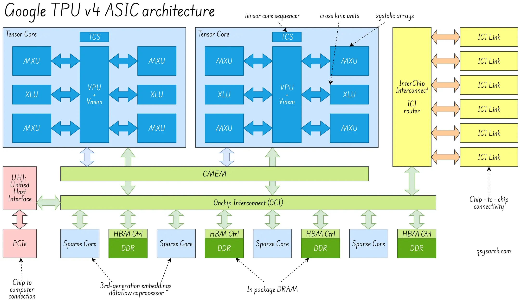
From the HW Connectivity perspective,
- The TPUv4 just like the TPUv2 and v3 are still using an Interconnect router (ICI), implemented as an high-speed electrical link between the TPUs within the same rack.
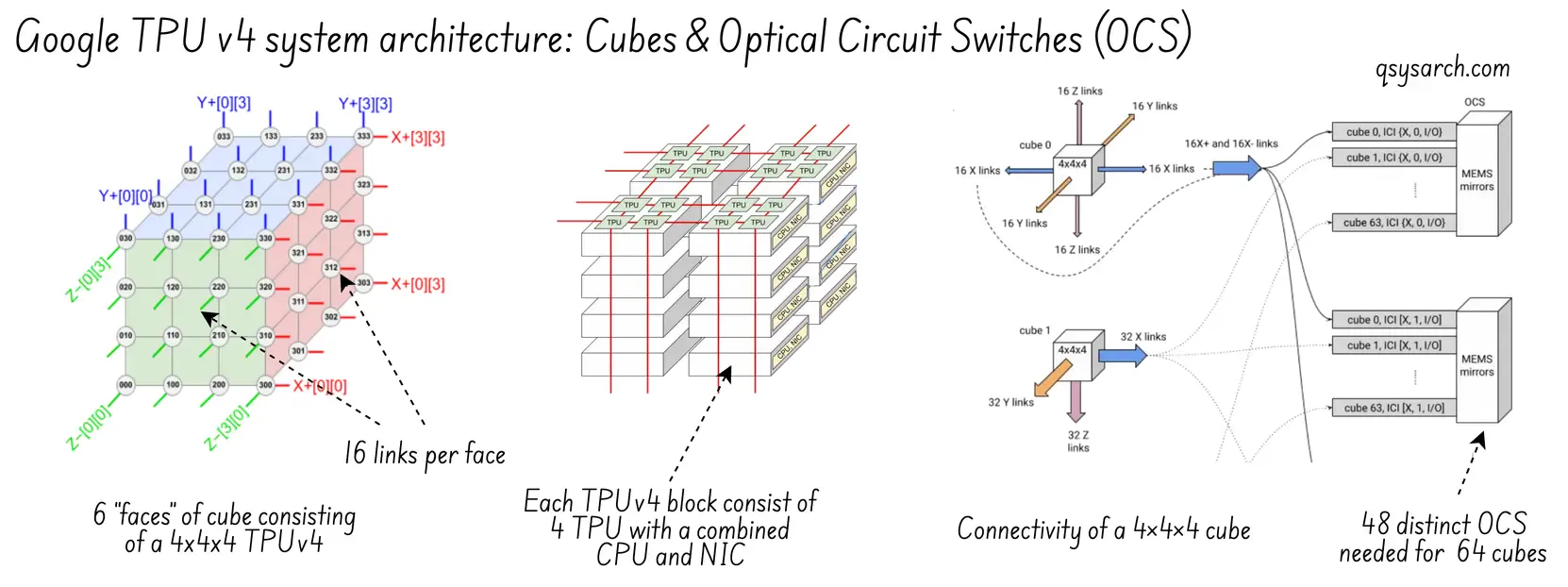
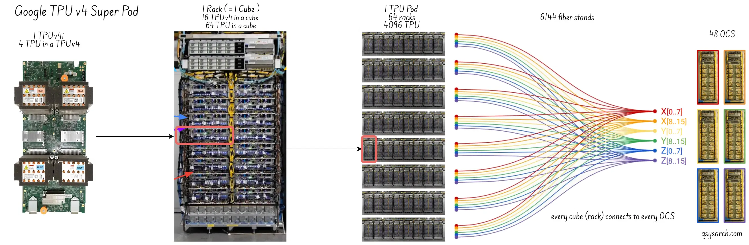
- However, the TPUv4 gets an additional Optial link between the racks, called Optical Circuit Switching, or OCS. This allows increasing the number of TPUs in a pod to 4K (compared to 64 in a single rack), as well as mitigating failures by reconfiguring OCS routing.
- Last, but the least, the routing now becomes 3 dimensionnal, by implemented a 3d torus, which has the non negligible advantange to scale the communication efficiency much better than the 2d torus.
From the SW perspective:
- Introduction of new tools: Borg as the cluster manager; pod manager to configure the OCS; and Libpunet to setup the ICI routing tables and cope with fault tolerance.
- Advanced single program multiple data (SPMD) compiler: This can be seen as a compiler generating multiple threads, where each thread is a program runing on a different TPU within the same rack or not. It is somewhat similar to the SIMT concept of the GPU, where the compiler generates code for the threads within a GPU warp.
- Since many TPUs are running the same program, the Borg orchestrator needs to make sure that all of the TPUs are cosynchrnous - that’s the role of the Gang Scheduler.
- Explain the concept of “pathways”, needed to handle asynchronous dataflow for MoE.
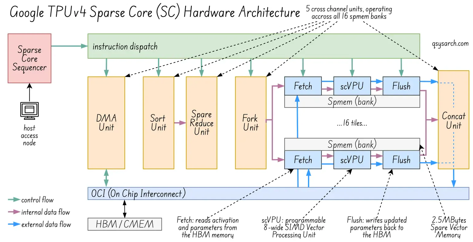
The SparseCore Link to heading
The SparseCore (aka SC) in TPUv4 is responsible for accelerating workloads with sparse matrix, where most of the values are zeros or redundant (which is the case for the embeddeings found in LLMs). It is described as an “embedding lookup” optimizer, and each TPUv4 includes four 4 SparseCore processors.
 (image adapted from the original image source)
The SparseCore Sequencer (in red on the top left corner) is the orchestrator responsible for disptaching instructions to the 5 cross channel units (in orange), as well as to the 3 “fetch/process/flush” SIMD units (in blue). Each SIMD units operate on their own 2.5MB tighly coupled memory scratchpad (in grey).
Given that each fetch/process/flush SIMD unit operates 8 data lanes at a time (SIMD=8), and that there are 16 of those SIMD units in a Sparse Core processor, that makes it a very powerfull processing unit, almost like a tiny GPU inside the GPU! Or to be precise, 4 tiny GPUs inside a TPU!
It would be really nice to have a look at the ISA used to program this powerfull SparseCore procesing unit, but I could not find any information online. It’s probably because it is more like a powerfull “Synchronous SIMD ALU-capable DMA computer” with so specific instructions that it only make sense to provide an higher level abstraction, such as the JAX library.
In practice, the user writes the high-level functional code, and the XLA (Accelerated Linear Algebra) compiler identifies patterns that match the SparseCore’s hardware capabilities.
import jax
import jax.numpy as jnp
from flax import linen as nn

# 1. Define the Embedding Table
# Imagine 1 million items, each represented by a 128-dimension vector
vocab_size = 1_000_000
embed_dim = 128

class SparseModel(nn.Module):
    @nn.compact
    def __call__(self, indices):
        embedding_layer = nn.Embed(num_embeddings=vocab_size, features=embed_dim)
        return embedding_layer(indices)

# 2. Input data (Indices)
# Note that index 105 and 42 are represented twice - GH the XLA compiler
# be able to tell the SC to only fetch 3 memory location, and not just 5?
input_indices = jnp.array([105, 42, 28, 42, 105])

# 3. Generate the actual TPU/SC code (well, that's called compilation!)
model = SparseModel()
params = model.init(jax.random.PRNGKey(0), input_indices)
output = model.apply(params, input_indices)
What happens under the hood? The method model.apply calls the XLA compiler, which lowers the code to the SparseCore. For this, it matches the nn.Embed (a gather operation), and generates the following “pseudo-instructions”:
- Dedup: XLA notices 42 and 105 appear twice in your input. It generates SparseCore instructions to deduplicate these before the fetch.
- DMA: Generates the SC-scalar instructions to calculate the memory offsets for IDs 105, 42, and 28.
- Push: Moves back the resulting 5*128 tensor into the Common Memory (CMEM).
The XLA compiler also need to take care of data placement. In particular, since the Sparse Core will need to access the nn.Embed indices, those indices need to be placed in a memory accessible by the sparse core. It could put it in the CMEM, but it is quite small (128MB), so it usually puts the embeddeing in the large HBM (32GB for TPUv4). The output of the Sparse Core processing is however put back in the CMEM, has it is only a slice of the data.
It is also worth noticing that the SparseCore architecture has evolved in the next v6+ generations.
MoE Mixture-of-Experts and Pathways Link to heading
The Mixture-of-Experts (MoE), unlike conventional …
The pathways concept refer to the physical and logical routes tokens take as they are sharded across experts living on different TPU chips.
 (
(2023 onward: v5, v6 (Trillum) and v7 (Ironwood) Link to heading
There is not much information available on the newer generations, so those are the big headlights:
- v5e: 16 GiB HBM3e per chip;
- v5p: 95 GiB HBM3e per chip;
- v6: 32 GiB HBM3e per chip; Improved BF16 performance
- v7: 192 GiB HBM3e ; New FP8 precision
With Ironwood v7, a super pod consists of ~9K TPUs.
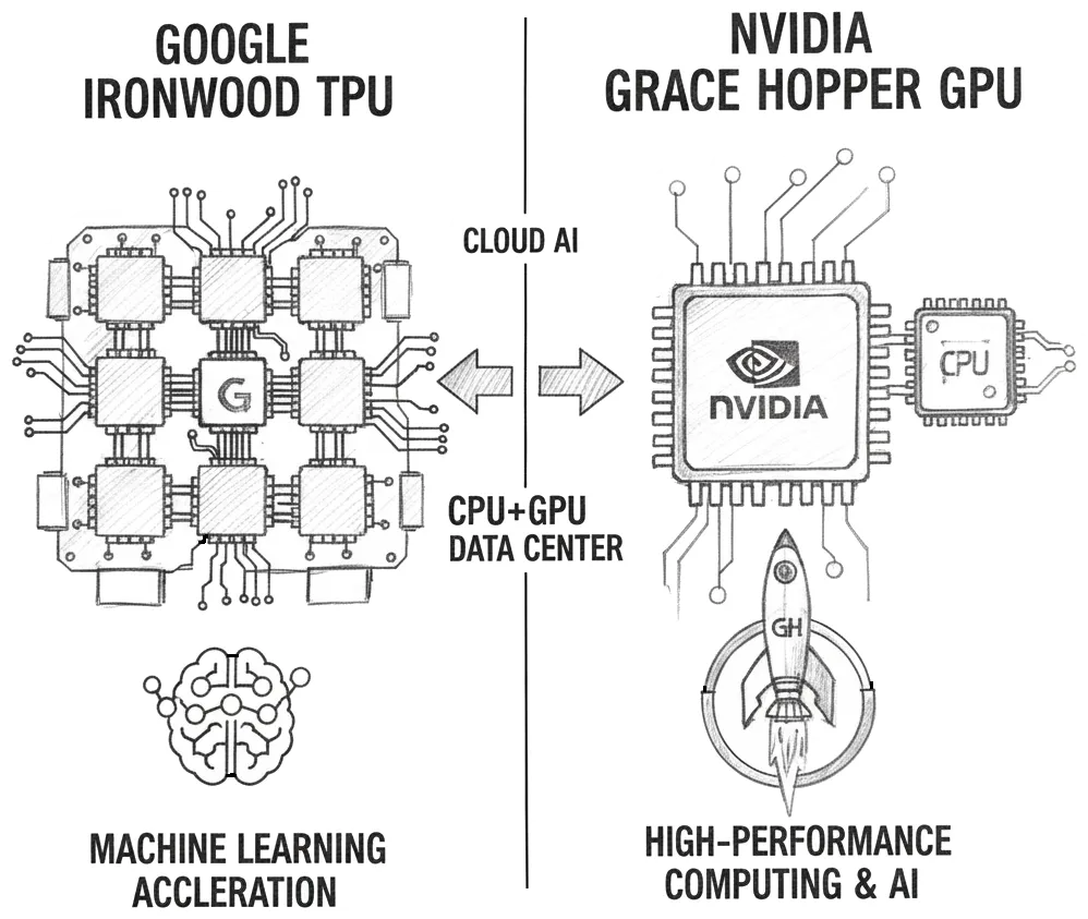
So, why do we still need GPUs if we have TPUs Link to heading
The TPU’s design, which balances memory, computing power, energy use, and data communication, shows that building high-performance AI systems at scale is not just about having fast chips. It also requires coordination between hardware, software, systems, and network connections.
Processing pixels vs processing matrices Link to heading
Even though AI workloads are more varied nowadays, covering inference, training, sparse models, and recommendation systems, TPUs are not designed to process pixels. GPUs, however, are not popular today because Nvidia exposed a programmatic model and developer experience that enabled GPUs to behave like a TPU.
![]()
Does this mean that GPUs are superior? Not necessarily - given very specific workloads, TPUs can be more efficient than GPUs, especially in terms of power consumption and performance per watt. And in the world we live in, where AI data centers consume ever more energy, TPU may make all the difference.
What about analog neuromorphic ICs? Link to heading
And what about neuromorphic ICs? Compared to TPU, they aim for even lower power consumption by using analog computing and lower-frequency event-driven processing. What will it take for neuromorphic ICs to become mainstream and reach the same scale as the TPUv7 super pods?
One of the challenges I still have is to better understand the relative power consumption of the systolic array (MXU + Spares Core) vs the rest of the TPU (including ICI, OCI, TCS), and how this ratio compares to the neuromorphic Spiking Neural Network (SNN) vs control logic (RiscV and Spike copro).
Also, if the Neuromorphic ICs were to reach the scale of TPUv7, it would likely require a similar level of investment in software, systems, and network connections. If not, one could consider plugging an SNN into a TPU and using the TPU’s “control logic” to handle communication between the SNN and the rest of the TPU/Rack/Pad. But is there a need for this? What problem are we solving? Maybe one needs to think differently.
Back to the future: the Language Processing Unit Link to heading
This memo would not be complete without mentioning the Language Processing Unit, a new type of processor designed to optimize the inference of large language models.
I will need to create a dedicated memo for this single topic, so for now, this is just a high-level comparison, trying to understand whether the LPU is more than a reinvention of the TPUv1, which was only focused on inference and not training.
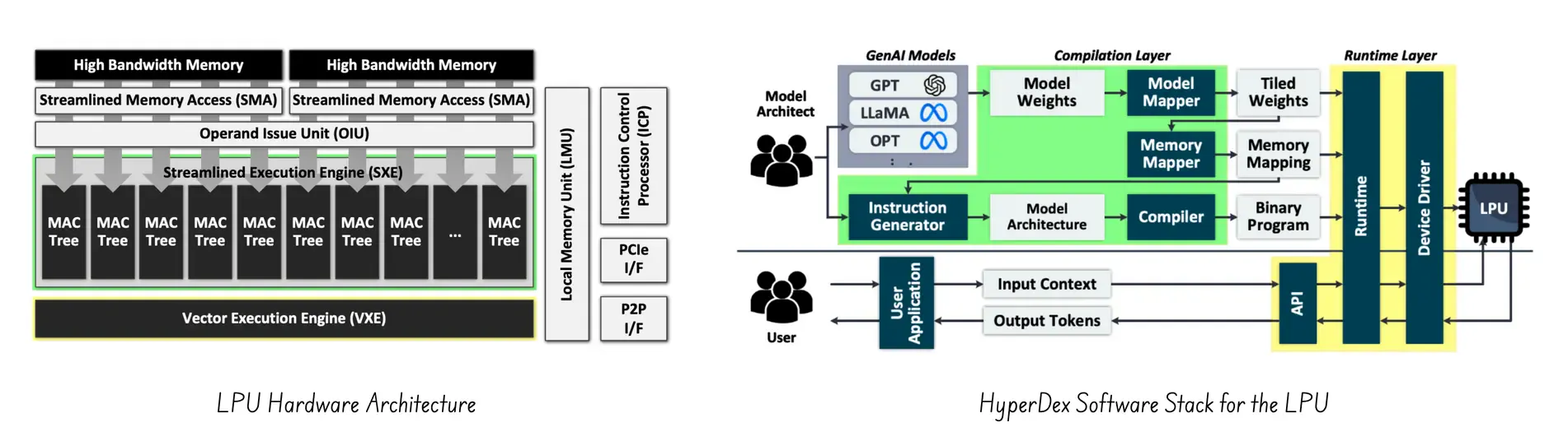
At a high level, yes, TPU and LPU share the need to do a few things very efficiently, and at scale, using a Domain-Specific architecture (DSAs). But when it comes to specific implementation and optimization, the LPU is a very different beast, with a different focus.

The main difference is that the TPUv1 was designed before the LLM even existed (remember, ChatGPT’s initial release was in 2022), and was focused on general Deep Neural Network (DNN) inference. That meant ensuring throughput and performance per watt for massive, high-volume operations, implemented by an underlying MXU systolic array.
The LPU, on the other hand, is designed to optimize the inference of large language models (LLMs). Their focus is on improving the latency per token. And for that, they need an ISA that supports a fully deterministic, statically scheduled, VLIW-based multi-pipeline architecture. Of course, one may argue that the TPUv4 introduces a similar VLIW ISA for the TCS. But the main difference is that the LPU ISA is a fully deterministic VLIW machine, where every load, compute, and store is scheduled cycle by cycle. While for the TPU, the MXU is a “self-driven” systolic array.
Conclusion Link to heading
Voilà, this is a short memo that, once again, took longer than expected. What is clear from this deep dive is that the evolution of the TPU architecture shows that designing AI accelerators is a complex task that requires balancing many factors.
The TPU’s design, which balances memory, computing power, energy use, and data communication, shows that building high-performance AI systems at scale is not just about having fast chips. It also requires coordination between hardware, software, systems, and network connections.
This is a bit of a feeling of déjà vu. Could it be that the Quantum Processing Unit (QPU) is the next step in the evolution of AI accelerators?
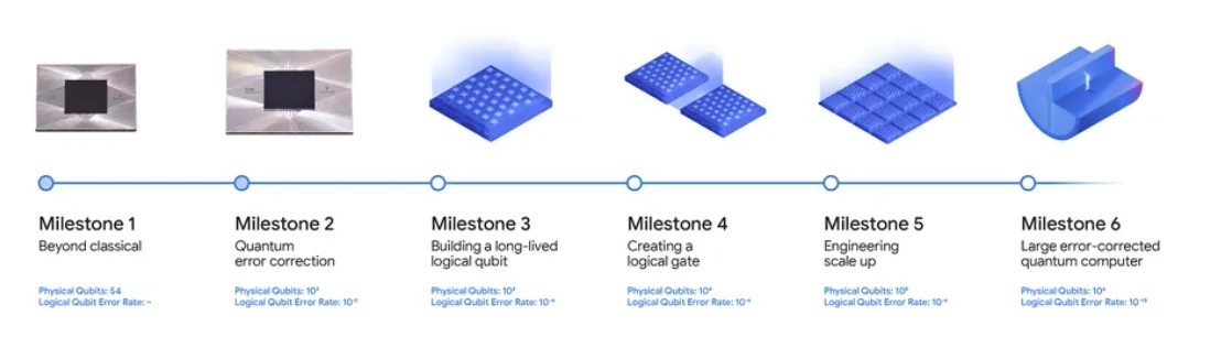 (image source: Google Willow)
References Link to heading
- An in-depth look at Google’s first Tensor Processing Unit (TPU)
- Touching the Elephant - TPUs: Understanding the Tensor Processing Unit
- TPU Architecture: Complete Guide to Google’s 7 Generations
- Tensor Processing Unit
- Why Google’s TPU Could Beat NVIDIA’s GPU in the Long Run
- LPU: A Latency-Optimized and Highly Scalable Processor for Large Language Model Inference
- TPUv2: A DomainSpecific Supercomputer for Training Deep Neural Networks
- TPU v4: An Optically Reconfigurable Supercomputer for Machine Learning with Hardware Support for Embeddings
- A Machine Learning Supercomputer With An Optically Reconfigurable Interconnect and Embeddings Support
- Resiliency at Scale: Managing Google’s TPUv4 Machine Learning Supercomputer
- TPU deep dive
- Ten Lessons From Three Generations Shaped Google’s TPUv4i
- How to Think About TPUs
- Google’s AI Processor’s (TPU) Heart Throbbing Inspiration
- Tensor Processor Unit (TPU)
- Raytracing & GLSL
DrawIO diagrams used in this memo: