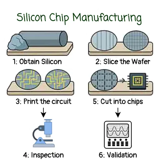
 This short memo summarises the methodologies used in semiconductor metrology, used for sillicon wafer inspection.
Semiconductor metrology involves the precise measurement and analysis of wafers used to produce ASICs. The objective is to ensure the quality and performance of atomic-scale transistor placement during device manufacturing, as even a pico-meter deviation in the manufacturing process would affect yield.
Metrology Technologies Link to heading
Here are some of the techniques and instruments used for quality measurements, along with an overview of their roles in the process:
Optical Microscopy (~2D)
 Link to heading
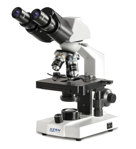
Traditional optical microscopes (used for biology) require light to pass directly through (“transmitted”) the specimen to detect phase shifts. However, silicon wafers are completely opaque and highly reflective. Because light cannot pass through a silicon wafer, those standard systems cannot be used.
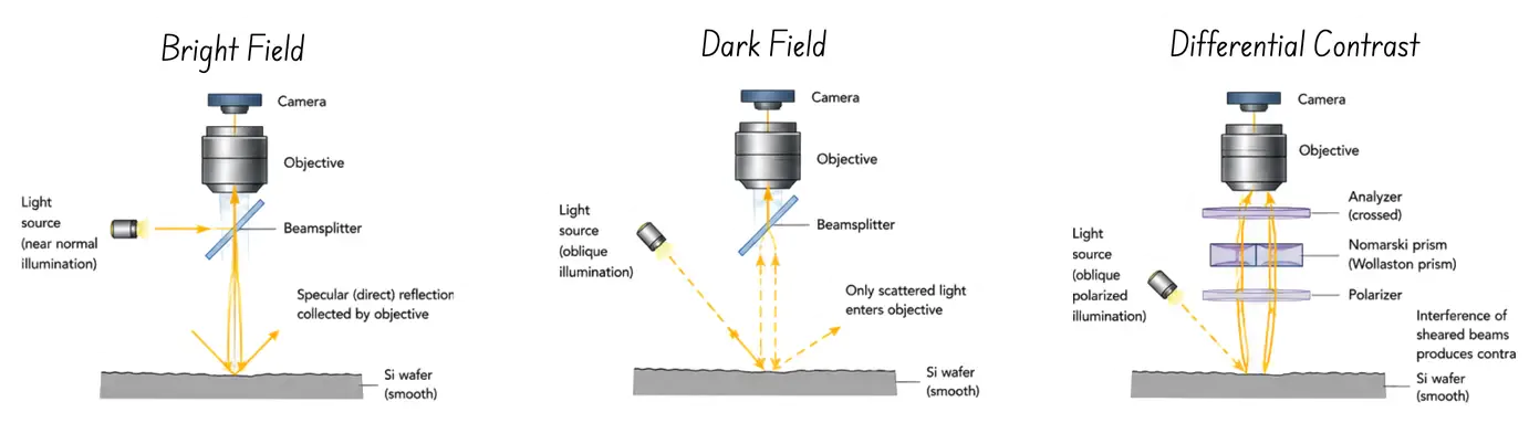
Instead, wafer inspection uses reflected light, with a few variants: Brightfield, Darkfield, and DIC (Differential Interference Contrast). Brightfield uses a light that shines straight down onto the wafer and reflects directly back up, while Darkfield uses a light that strikes the wafer at a steep, oblique angle, which can be used to detect any raised defects such as particle contamination, hairline scratches, and micro-defects.
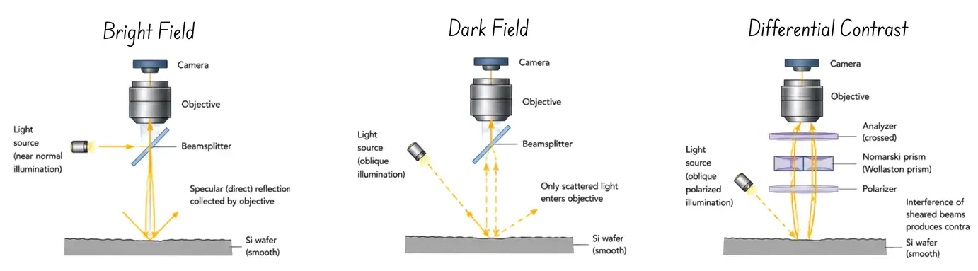
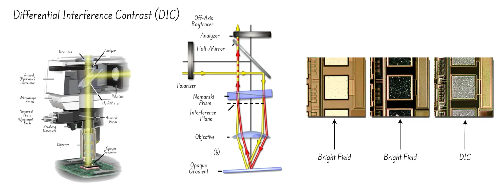
The most interesting for wafers is the Differential Interference Contrast microscope, which uses polarised light and a specialised Wollaston prism to split light into two paths, bounce them off the surface, and recombine them. It can be used to reveal microscopic height differences and surface textures by giving the wafer a 3D-like observation.
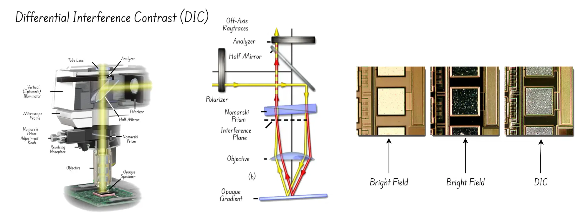 (image source: Nikon Microscopy)
Scanning Electron Microscopy (SEM)
 Link to heading
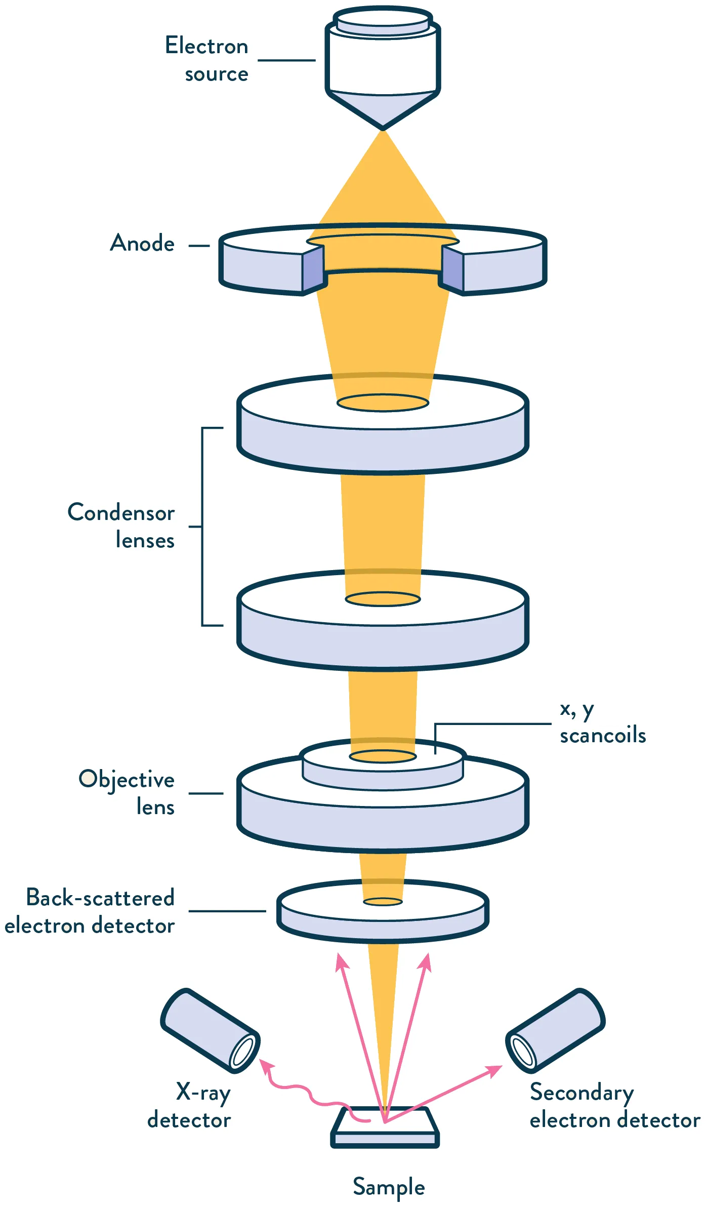
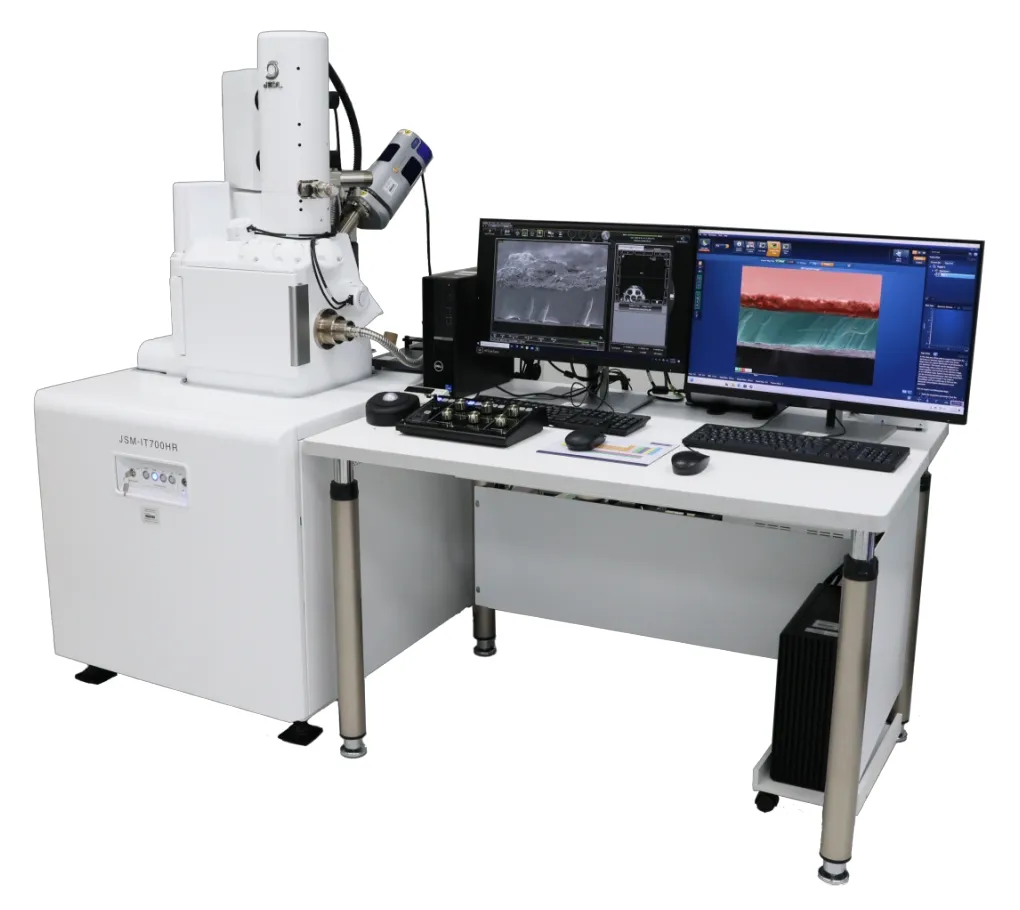
Scanning Electron Microscopy (SEM) is one of the most common instruments used in semiconductor manufacturing due to its ability to observe much smaller features than optical microscopes (100 times higher resolution). Instead of light, SEM uses a focused beam of electrons to scan the wafer surface, enabling it to produce high-resolution, 3D-like images of its topography and composition.
Unlike the optical microscope, which can take a “picture at once,” the SEM needs to “scan” the wafer point-by-point with a very fine electron beam and then reconstruct the image, with each pixel’s brightness depending on the number of electrons detected from the corresponding location on the wafer. The scanning does not use mechanical parts, but rather magnetic coils that generate fields that focus the electron beam into a spot only a few nanometers wide (somewhat similar to old and bulky CRT televisions)
Atomic Force Microscopy (AFM)
 Link to heading
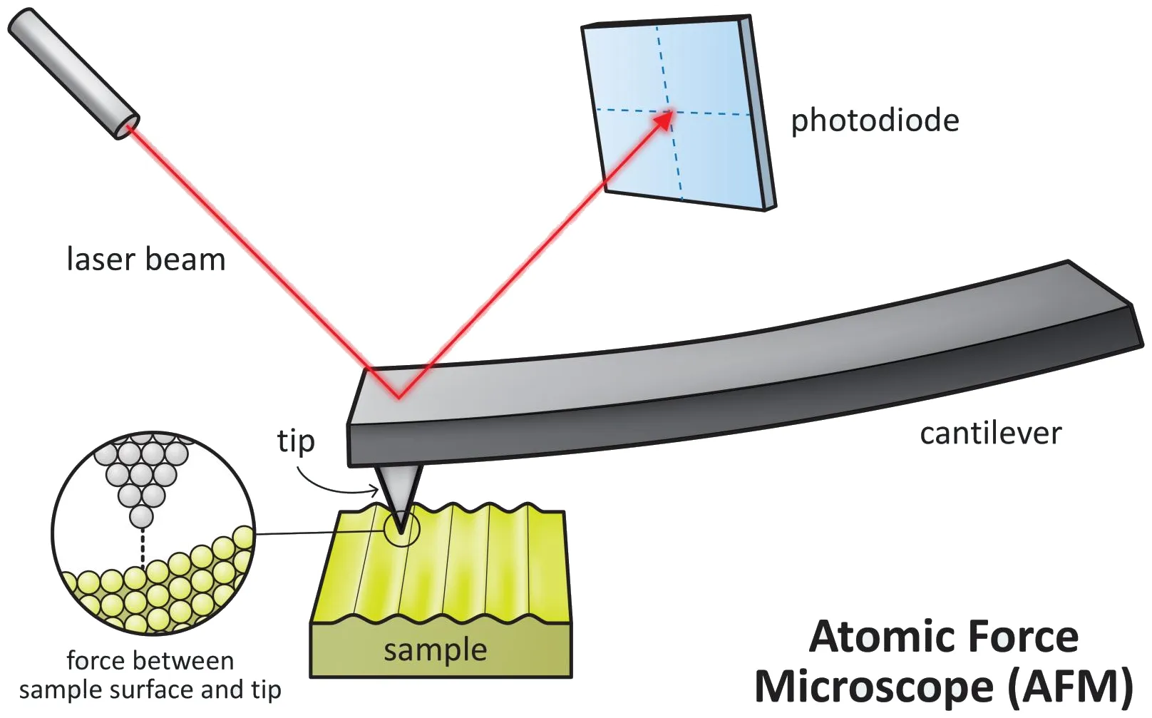
Atomic Force Microscopy (AFM) is fundamentally different from SEM: rather than using electrons, it uses an ultra-fine tip on a flexible cantilever to “feel” and map the topography of a surface at the atomic scale, much like a blind person reads Braille. An AFM measures surface topography.
Like an SEM, the AFM scans the surface point by point. However, instead of recording emitted electrons, AFM measures multiple parameters, including tip height, cantilever deflection, and interaction force, resulting in a true 3D surface map.
The cantilever can interact with the observable in multiple modes: In contact mode, the tip remains in continuous contact with the wafer. In tapping mode, the cantilever oscillates near its resonant frequency, and brief contacts with the surface modify its oscillation amplitude. There is also a non-contact mode which uses attractive forces as the measurement principle, but that is also more prone to a lower signal-to-noise ratio.
X-ray Diffraction (XRD)
 Link to heading
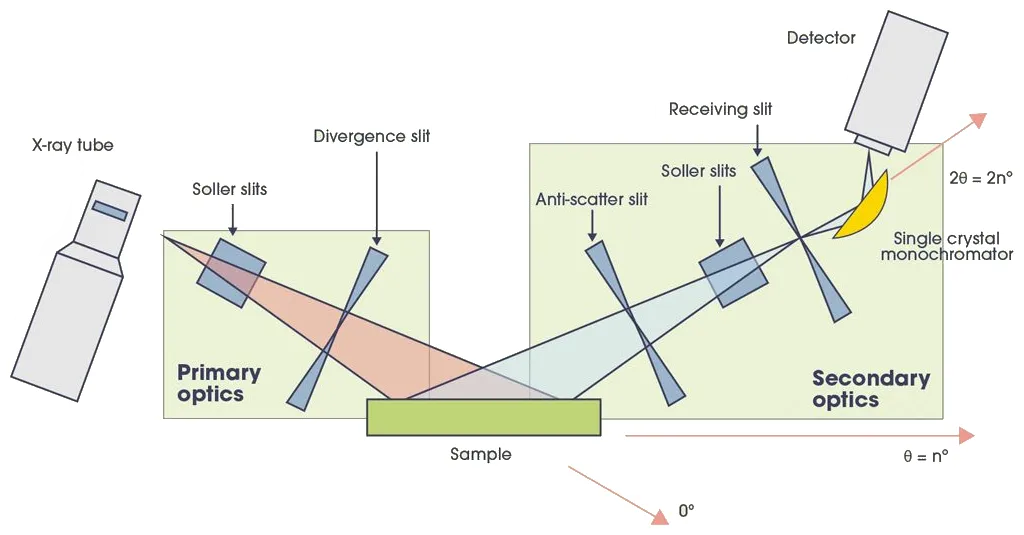
X-ray Diffraction (XRD) is very different from previous instruments, which mainly examine the surface of a wafer, whereas XRD probes the crystal (or atomic) structure inside the material.
It is one of the most important non-destructive measurement instruments for determining whether a silicon wafer has the correct crystal orientation, lattice spacing, strain, and crystalline quality. XRD is indispensable because even if a wafer looks flawless under a “surface microscope”, subtle changes in the crystal lattice detected by XRD can significantly affect transistor performance and manufacturing yield.
Summary Link to heading
| Method | # | Resolution | Speed | Cost | Typical Use |
|---|---|---|---|---|---|
| Optical | ~ 2D | ~0.2 µm | Very fast | Low | Routine wafer inspection |
| SEM | ~ 2D | 1–10 nm | Slow | High | Detailed defect analysis |
| AFM | 3D | <1 nm (vertical) | Very slow | High | Surface roughness measurement |
| X-ray | 3D | Varies | Moderate | High | Internal structure inspection |
Atomic Force Microscopy high-level concepts Link to heading
The second part of this memo is on NearField Instrument, a TNO spin-off and now scale-up part of the European semiconductor ecosystem. Their most recent product, called QUADRA, is an Atomic Force Microscopy system.
High Level System overview Link to heading
The diagram below is a naïve and high-level representation of the QUADRA system.
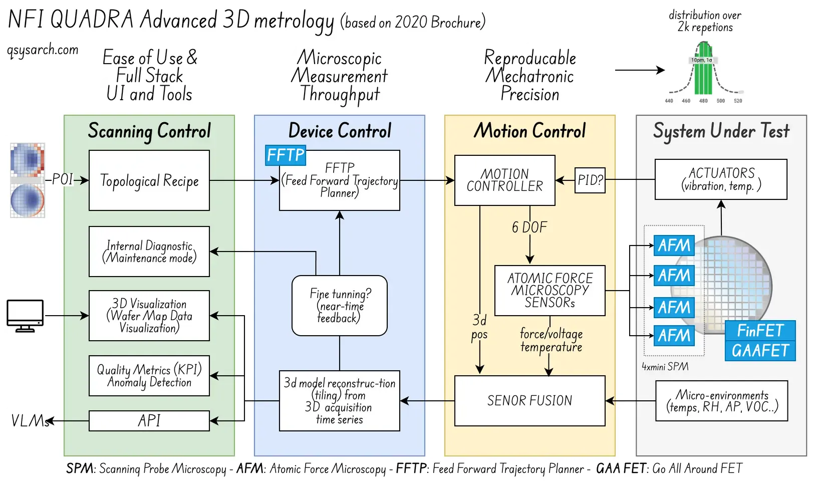
There are a few things worth noticing:
Heat Control: The AFM is extremely sensitive to temperature fluctuation around the probe. So, the less heat the tip motion control system generates, the better.
Scan Lining vs stitching: Newer systems have evolved from a traditional stitched set of tile measurements to full scan-line and uninterrupted wafer measurement.
Fine-tuning: Even if the system needs continuous fine-tuning, the key is that it generates extremely reliable and reproducible data, so learning can become predictable.
Performance (Latency): Given the tremendous amount of data to be processed, performance for data transfer, measured as latency, is essential to optimal operation.
Data Insight and drilling: QUADRA produces a lot of data, so the system needs to be operated around KPIs. For each KPI, the user should be able to drill down into specific measured data.
Mechatronic High-Level Overview Link to heading
The QUADRA mechatronic design is based on miniaturised AFM (MAFM) probes: Each QUADRA system has 4 MAFM, and each MAFM has its own positioning unit (PU) arm to be able to reach the independent locations of the wafer.
For AFM to be accurate, it is very important to reduce mechanical noise. For this, QUADRA uses an inverted architecture, where the wafer is vacuum-clamped on a chuck, and the tip approaches its surface from below (see diagram below). This allows shortening the mechanical loop and reducing noise from mechanical resonances by removing excitation points.
Switchable Kinematic Connections Link to heading
The shortening is achieved by switching the MFAM kinematic connection from the PU to a grid plate: the grid plate is a very stable nearby reference surface for the AFM. Once the AFM measurement head locks onto it, the cantilever’s position is defined relative to that local reference instead of the larger machine structure. This reduces mechanical errors and improves measurement accuracy.
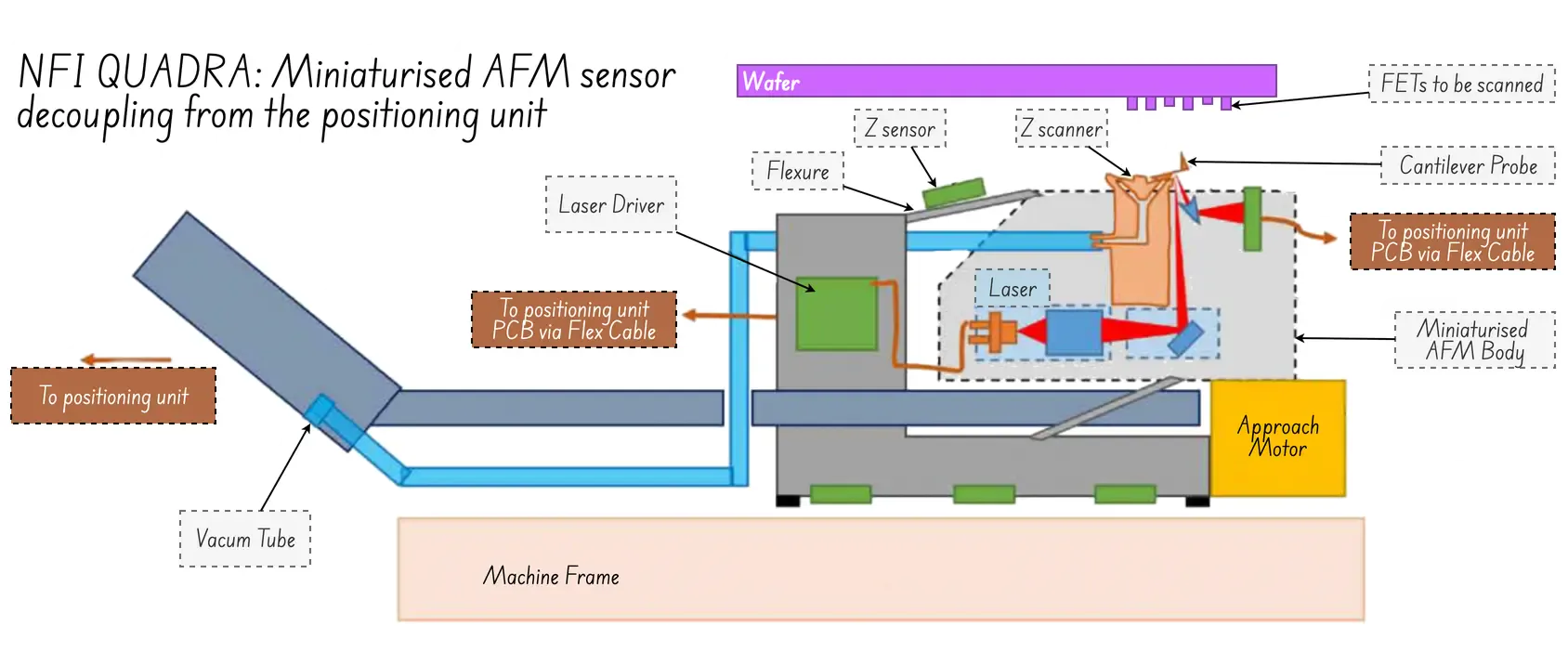 (image source: 2024 NFI brochure )
Lighting Mode Link to heading
As explained before, typical AFM instruments use tapping mode. QUADRA has a new innovative mode called Lightning mode, which can produce high speed scan up to 1 MPix/s (mega pixels per second). This mode is based on 3 pillars: An advanced Z-scanner control algorithms allowing for exploiting the full mechatronic bandwidth of the Z-scanner for tracking topography; An active control of fast-reacting cantilevers allowing the cantilever acting as the sensor to react to topography changes quickly (aka feedback loop); And last, but not least, a smart data-fusion algorithms where multiple signals from the MAFM are combined to reconstruct the topography image.
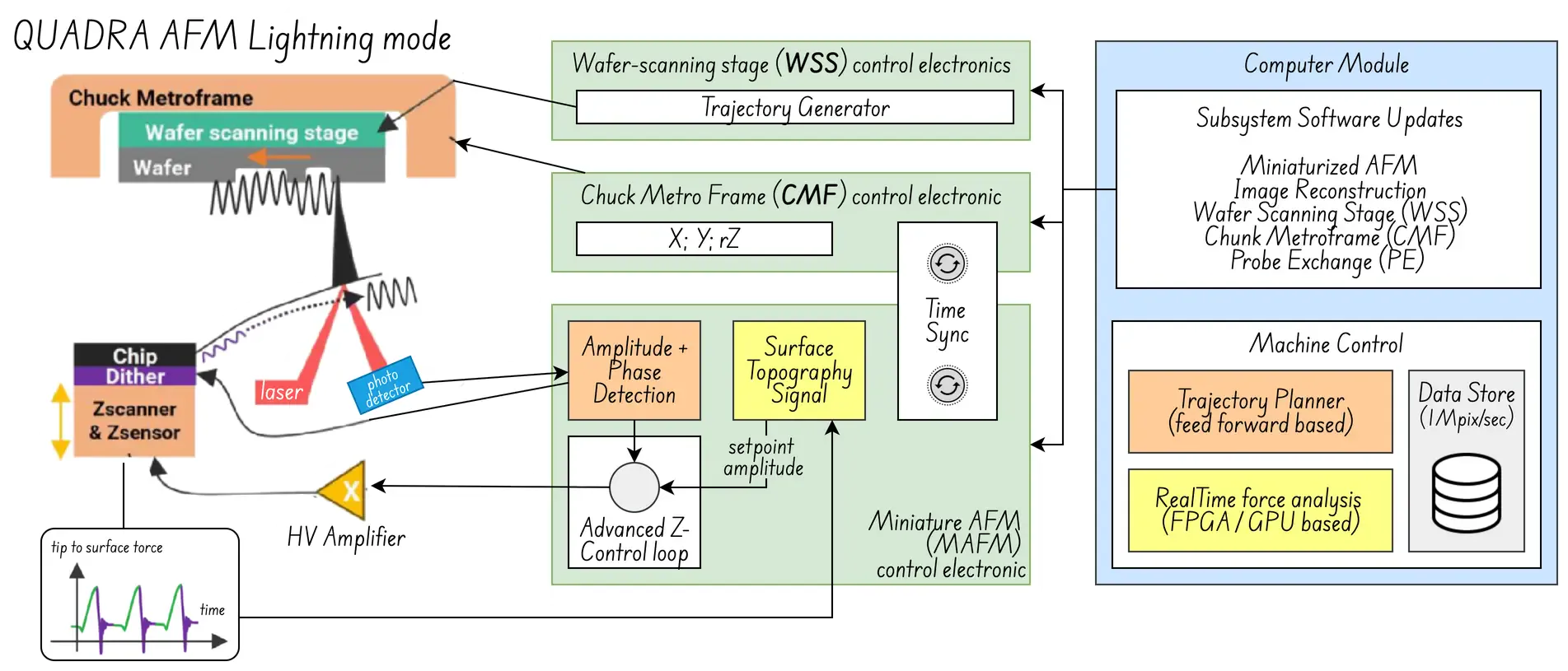
For more information, check the NFI QUADRA insightful paper
Semiconductor Verification: Chiplet-based SoCs Link to heading
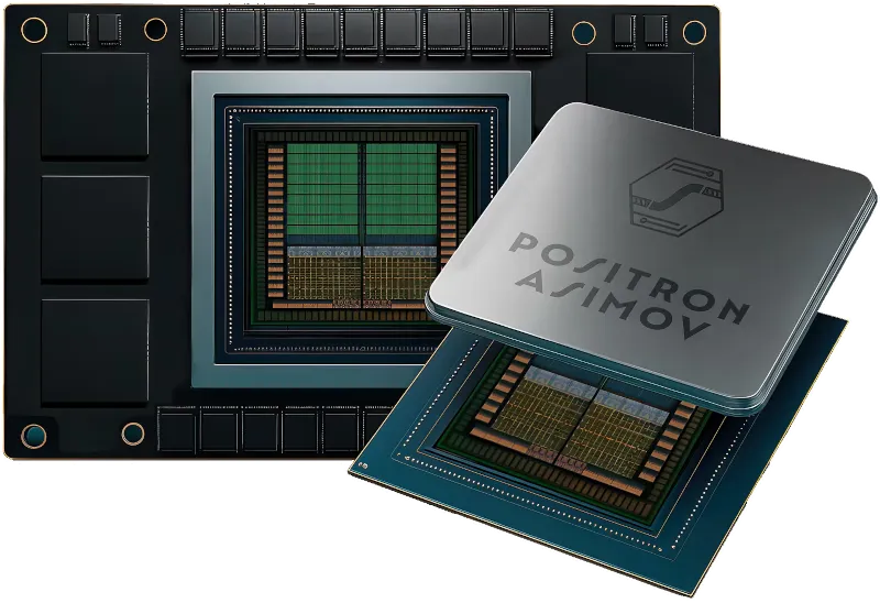 With such a powerful QUADRA system, it becomes possible to verify, among others, the Positron’s Asimov chiplet-based SoC.
Those are a few of the items that ought to be verified:
- Packaging Bonding: Chiplets rely on ultra-fine pitches (5–50 µm microbumps or sub-micron direct copper-to-dielectric). AFM can be used to measure picometer-scale topography maps of the surface;
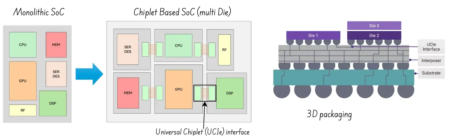
Electrical Nanoprobing: Because chiplets are packed closely together in 2.5D or 3D architectures, traditional testing probes cannot physically reach the internal interconnects. Conductive AFM (C-AFM): C-AFM passes a current through an ultra-sharp conductive tip to map localized electrical variations (*NDLR: I am not sure if QUADRA support C-AFM).
Dopant Profiling: A core benefit of a chiplet SoC is mixing nodes (e.g., a 3nm logic chiplet paired with a legacy 14nm I/O chiplet). AFM systems equipped with Scanning Capacitance Microscopy (SCM) map active carrier concentrations and dopant profiles across different semiconductor materials. This verifies that the processing nodes meet their target electrical characteristics after undergoing packaging-induced thermal cycles.
Interfacial Stress: Integrating materials with different coefficients of thermal expansion (CTE) can lead to warpage, delamination, or thermo-mechanical stress. AFM measures the elasticity, hardness, and adhesion at the interfaces of the chiplet, interposer, and silicon bridge.
Thermal Characterization: AFM tip with a built-in micro-thermocouple (aka Scanning Thermal Microscopy, or SThM) can map microscale thermal boundaries and track hotspot dissipation paths, ensuring that the SoC’s complex layout does not lead to destructive localized overheating.
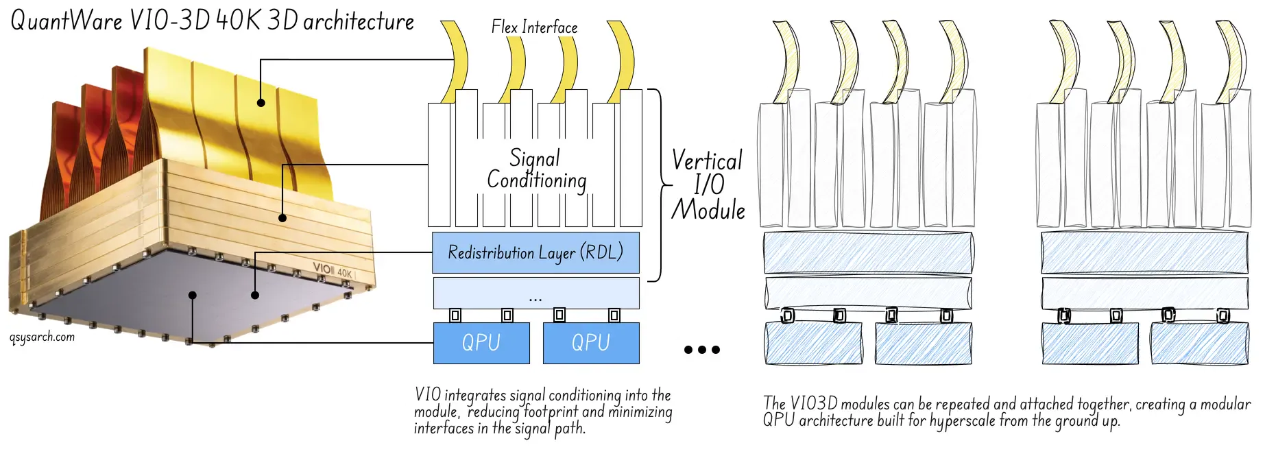
A more interesting question is how QUADRA could be used to ensure the advanced packaging and hybrid bonding of Quantware VIO-40K’s 3D architecture. I’ll keep this for a later memo.
Conclusion Link to heading
Voilà, this was another super short memo, and I hope it helps the reader better understand the challenges and possible solutions in silicon wafer metrology.
The interesting thing is that given the progress and activity in innovative AI inference ASIC, scaleups dealing with silicon metrology have a bright future ahead!
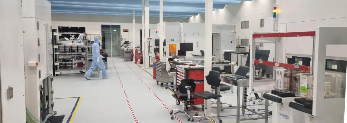 (A clean room - source: NFI)
References:
- Near Field Insturment QUADRA system
- Thermofischer Semiconductor Advanced Logic Transistor Analysis
- DEVELOPING A MINIMUM VIABLE PRODUCT THROUGH AGILE SYSTEMS ENGINEERING
- QUADRA: METROLOGY FOR THE ONGOING EVOLUTION OF MOORE’S LAW
- Review of chiplet-based design: system architecture and interconnection
- Wafer defect detection by a polarization-insensitive external differential interference contrast module
DrawIO diagrams used in this memo: