Before diving deep into the fantastic world of Quantum Error Correction, I thought it would be useful to have a short memo explaining how QPUs are architected, and in particular, how 1- and 2-qubit gates are implemented at the hardware silicon level.
The challenge in writing such a memo is that there are many QPU architectures, or modalities, so I will start with one of the common modalities: the superconducting Transmon qubit.
For reference, the image in the top right is Fairchild’s 4-transistor IC from 1961. At first glance, today’s transmons may seem as complex as this IC. In practice, it feels like the quantum industry is back where the silicon industry was in 1960, with an additional cryo+superconductivity factor. The exciting part here is to forecast the possible control logic evolutions based on what happened in the 70’s.
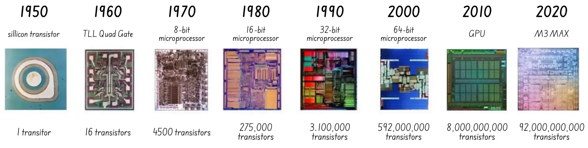 (image credit: Computer History Museum)
Transmon QPU blueprint Link to heading
The diagram below shows the components involved in an imaginary 2-qubit tunable transmon. The reason for using a 2-qubit architecture is that it allows for both controlling individual qubits (single-qubit gates) and entangling multiple qubits (two-qubit gates).
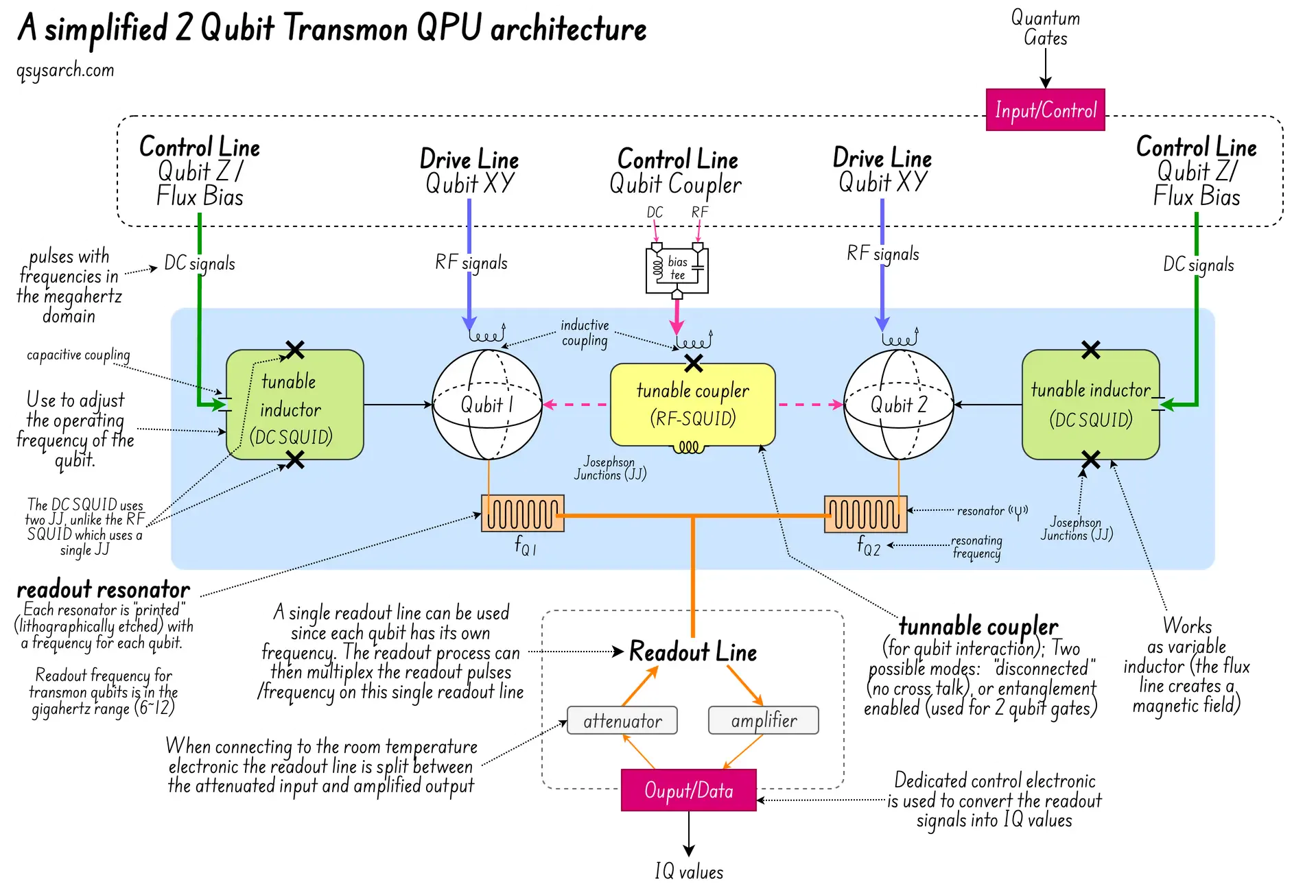
The “5 lines” on the top are used to control (manipulate) the qubit state as well as the interaction between the two qubits. The line(s) at the bottom are used to perform the qubit readout (i.e. collapsing of the qubit wave function, which is a destructive process).
Note that the above diagram assumes the transmon architecture is tunable, but this is not always the case; some architectures do not use tunable qubits, such as the OQC Coaxmon architecture.
One important factor in designing a transmon qubit is that it operates at a superconducting temperature, where the use of the Josephson Junction (aka JJ) makes it possible to control it without heat dissipation. I will skip the entire digression on the JJ and how it makes the Superconduction Quantum Inference Device possible. The interested reader can refer to the Superconductivity: SQUIDS video.
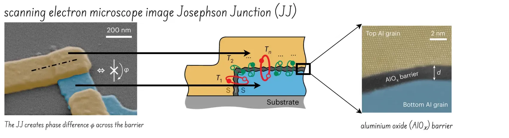 (image credit: Observation of Josephson harmonics in tunnel junctions)
Qubit Control Process Link to heading
Each control line carries a different type of signal, so the parts used, like dampers (attenuators) and filters, are different depending on whether you are handling the Drive Line, the Coupler Control Line,or the Qubit Control Line.
1. Drive Line (XY Control) Link to heading
For transmon Qubits, the XY drive line manipulates the qubit via weak capacitive coupling of microwave pulses (4–6 GHz). It functions as an on-chip antenna, applying an oscillating electric field to drive rotations on the Bloch sphere.
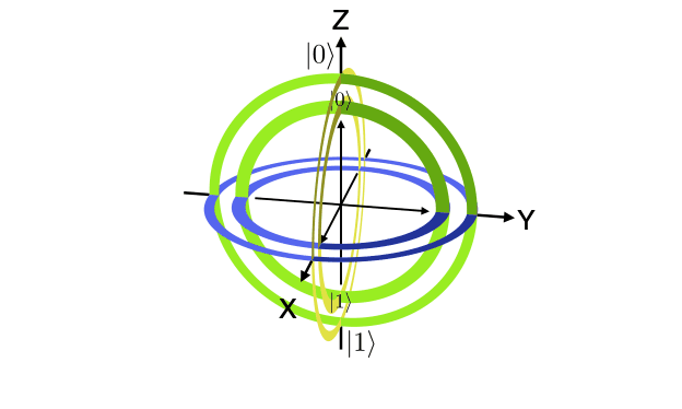
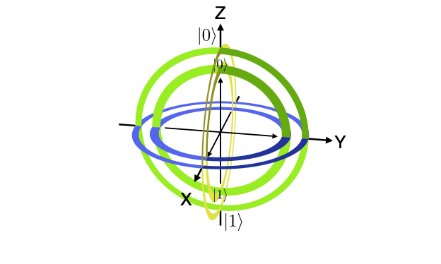
The XY drive line distinguishes between an X-gate and a Y-gate by varying the phase Φ of the microwave pulse, rather than its frequency or physical path. Because both gates require the same frequency (matching the qubit’s resonant frequency), the hardware controls the rotation axis by shifting the microwave electric field’s alignment relative to the qubit.
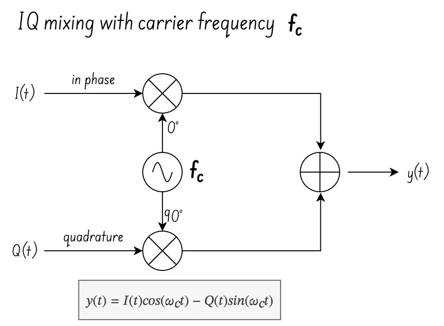 The alignment shift, or phase, is done with the IQ mixers, usually sitting with the other room-temperature control electronics. The IQ mixer uses IQ modulation of an in-Phase (
I) and the quadrature Q signals, together with a carrier frequency fc corresponding to the qubit resonance frequency. (image on the right based on Pulse Lib).
To create an X-gate, the control module, such as Qblox QCM-RF, just needs to set the I channel to full ON and keep the Q channel OFF. To create a Y-gate, it instead needs to turn the I channel OFF and turn the Q channel fully ON. Of course, it is much more complex in practice, and one needs to ensure that IQ mixer calibration is done to prevent leakage between X and Y gates.
2. Qubit Control Line (Z / Flux Bias) Link to heading
The flux bias (Z) control line is used to adjust each Qubit Frequency. This is done by changing the magnetic flux threading the qubit’s SQUID loop. The purpose of this line is threefold:
Pauli Z gate: by pulsing the Flux Bias control line, a Pauli Z gate is achieve by shifting the qubit’s frequency away from its idling frame for a gv duration, accumulating a precise phase difference (θ) relative to the computational frame.
controlled-Z (CZ) gate: For two-qubit operations, such as the controlled-Z (CZ) gate, a fast flux pulse temporarily shifts one qubit’s frequency to bring it into resonance with a specific energy level of a neighboring qubit, activating their interaction.
Idle protection: The flux bias line is also used to dynamically “park” qubits at specific, stable frequencies—often called “sweet spots”—where they are least sensitive to flux noise.
Note that physical pauli Z gates are rarely used because flux pulses introduce noise and can degrade coherence. Instead of sending a physical pulse, higher-level quantum circuit compilers mathematically shift the phase of subsequent XY microwave pulses. This is called Virtual-Z gate.
Qubit Readout Process Link to heading
1. Frequency Multiplexing: Why every readout resonator is unique Link to heading
Instead of running a separate, bulky microwave cable down into the dilution refrigerator for each qubit, multiple qubits are connected to a single common readout feedline (like a “bus” in traditional microarchitecture).
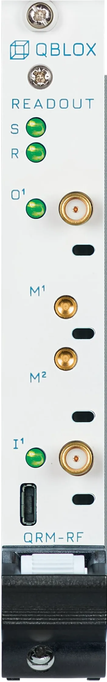
To avoid mixed signals, each qubit’s readout resonator is assigned a distinct frequency, spaced 30 to 100 MHz apart within the 6 to 8 GHz range. A room-temperature AWG/pulsar (like the Qblox QRM) is used to send a pulse composed of a mixture of all those individual frequencies down the line (up to 6 frequencies at the same time).
Each qubit resonator only interacts with its own specific frequency, ignoring the others. When interacting with the qubit, the resonator generates an echo at a frequency similar to the input frequency. All of the echoes are collected simultaneously by a room-temperature pulsar, which decodes them in parallel.
This single readout channel acts like a bus for sending and receiving frequency-multiplexed pulses.
2. Measuring the qubit state: The dispersive shift Link to heading
While the readout’s resonator’s physical frequency is fixed, its effective (“reflected”) frequency changes dynamically by a tiny amount depending on the qubit state. This is called the dispersive shift.
When the qubit is in state
|0>, the resonator responds at frequencyf0.When the qubit flips to state
|1>, its quantum interaction pulls the resonator’s frequency slightly, causing it to respond at frequencyf1
The readout line isn’t dynamically tuned by an external flux line, as in a DC SQUID. Instead, room-temperature computers perform Resonator Spectroscopy during calibration to map out these exact printed frequencies. They find the precise peak response for each qubit’s |0>. The diagram below show the process of sweeping around the resonating frequency to identify the peak resonator frequency.
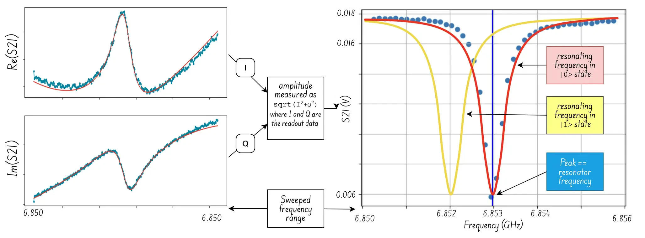 (Image source: QBlox and ENCSS).
Performing resonator spectroscopy using the Qblox Scheduler is as simple as those few lines of Python code. For more information, check the online tutorial.
spectroscope = Schedule("resonator_spectroscopy")

sweep_frequency_domain = linspace(
    start=frequency_center - frequency_width / 2,
    stop=frequency_center + frequency_width / 2,
    num=frequency_npoints,
)

with spectroscope.loop( sweep_frequency_domain ) as freq:
    spectroscope.add( Measure("Q0", freq=freq, coords={"frequency": freq}, acq_channel="S_21"))
    spectroscope.add(IdlePulse(10e-6))  # Let the resonator decay

# Execute the experiment
sweeped_iq_readout_data = hw_agent.run(spectroscope)

# Generate the above graphs automatically
ResonatorSpectroscopyAnalysis(rs_data).run().display_figs_mpl()
Note that the IdlePulse is used to let the resonator decay between measurements so that the electromagnetic energy from the previous probe pulse completely dissipates (“thermal reset”). It is also used to ensure measurement independence and prevent spectral distortion (“no memory effect”).
Qubit Entanglement Process Link to heading
Tunable Coupler Control Line Link to heading
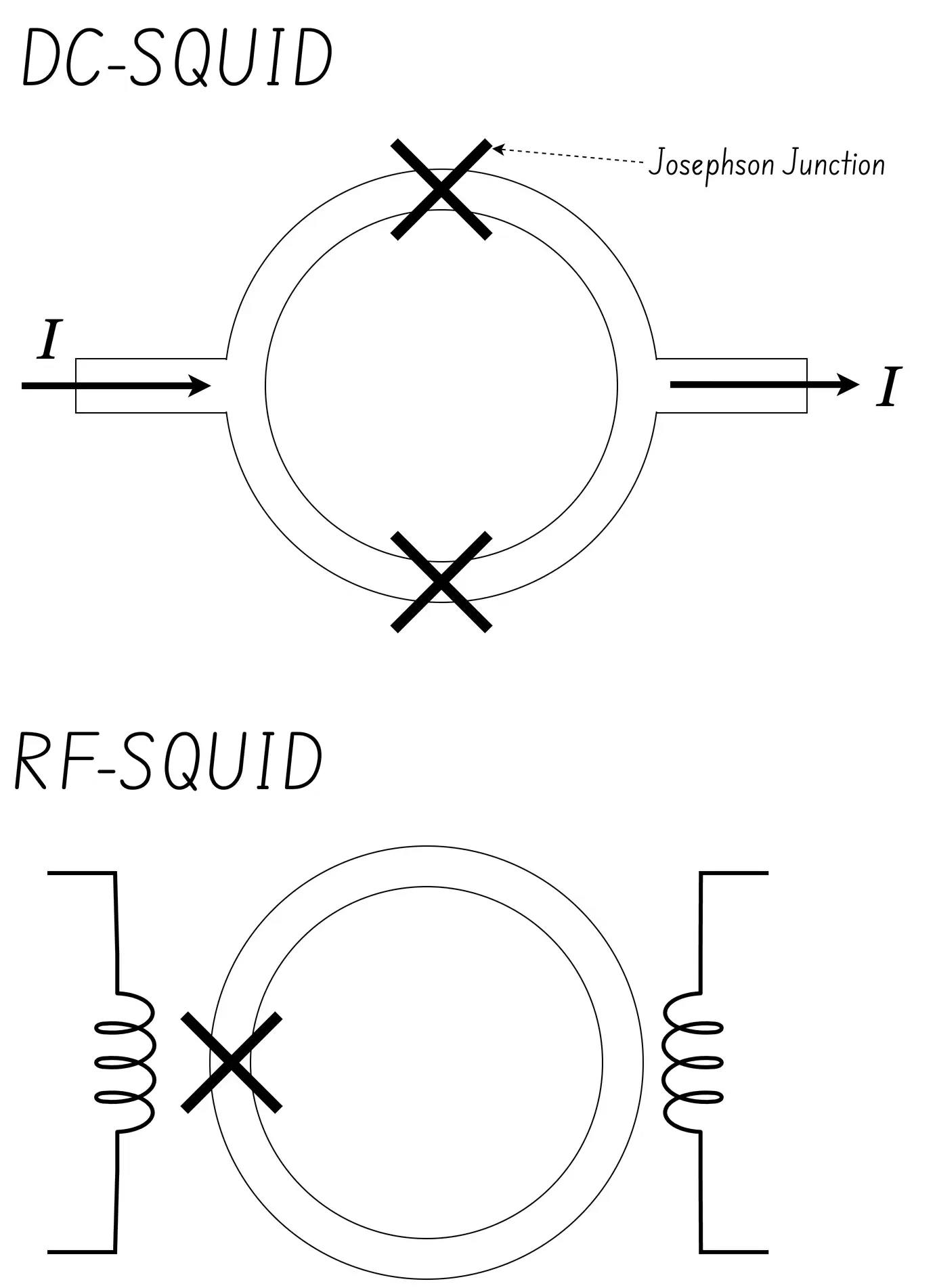 At a glance, the tunable coupler, implemented as an RF-SQUID, acts as a loop in which one injects magnetic flux, altering the coupler's effective inductance and resonance frequency, which in turn nonlinearly changes the interaction strength between the qubits.
No discrete electronic components (like standard commercial resistors, capacitors, or coils) are placed near the RF SQUID on the QPU chip. The Reason is that standard electronic components generate heat, introduce electrical noise, and fail to function properly at the QPU’s dilution refrigerator operating temperature of 10 millikelvin.
How it’s built instead: The entire control mechanism is monolithically integrated. The flux line is lithographically etched directly onto the silicon using the same superconducting metals (such as Aluminum or Niobium) as the qubits themselves.
Performing 2 Qubit Gates Link to heading
The 2-qubit gates are an indispensable component of a universal gate set for quantum logic. By controlling the shape of the pulses sent to the tunable coupler, the RF SQUID enables two primary types of entangling gates:
Controlled-Z (also known as CZ or CPHASE): The 2 qubits only experience a phase shift if both qubits are in the
|1>state (transform the state|11>into-|11>)).iSWAP : The 2 qubits swap their quantum populations (e.g., exchanging
|01>into|10>).
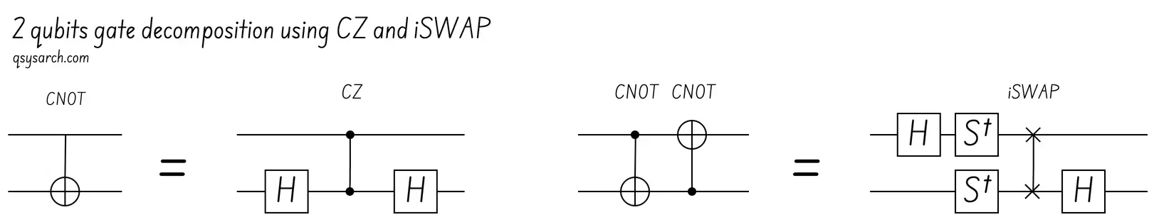
Note that those gates are symetric, meaning that Q₁ CZ Q₂ ≡ Q₂ CZ Q₁, resp iSWAP. Non-symmetric gates like CNOT can be built using a composition of those symmetric gates and single-qubit gates. For example:
Generating Gates from Pulses Link to heading
There is a lot to unpack about how the RF-squid works and what kinds of pulses are needed to create the different gates, and this could be the topic of a memo alone. At a glance:
Predistortion: the cables and filters leading into the cryo are distorting the electrical signals; So, the pulses needed to be “predistorded” by the room-temperature pulsar (in software/FGPA) to make sure the perfect shape is received by the time it reaches the coupler.
faster gate time vs gate fidelities: To overcome the short qubit coherence time, researchers are trying to make faster gates. The challenge is the fidelity, or leakage to noncomputational states (e.g.,
|02>): The common approach is to shape pulses using derivative removal by adiabatic gate (DRAG)
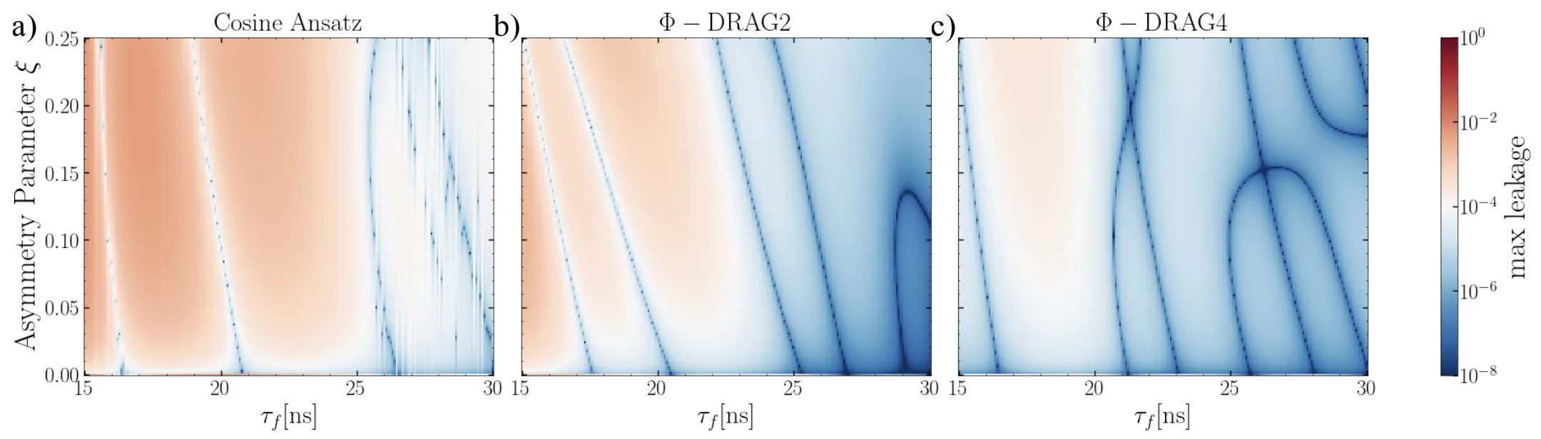
image credit: arxiv.org/2606.13052; What is important to notice is that the leakage increases as the gate time decreases, and that carefully shaping the Φ-DRAG-x can further reduce the leakage;
In practice: From paper blueprint to real hardware Link to heading
In practice, creating a real silicon for a transmon qubit is slightly more complex. The image below (credits: Anuj Aggarwal) shows a 5-qubit transmon silicon die. One of the tricky question is how can one do a native three qubit gates, such as the Toffoli gate (also called the CCNOT), with such hardware, without breaking down to multiple 2 qubit CNOT gates. I’ll keep this question for a later memo.
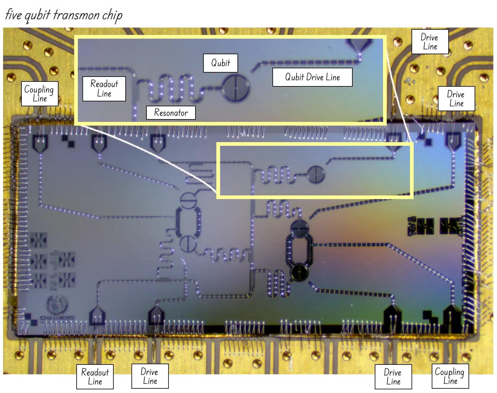
While looking for QPU silicon die pictures, I noticed it is surprisingly difficult to find photos with sufficient detail to understand their connectivity. This is very likely because those photos can reveal critical details about cross-talk mitigation strategies that QPU manufacturers are patenting. Innovative solutions, such as the VIO-3D from Quantware, use vertical channels to further reduce this cross-talk.
The next challenge is to get the QPU hardware above in a cryo environment in which the superconducting property of the Josephson Junction (among others) can be exercised. The image below hints at what needs to be done. Bluefors is a major player and leader in this domain.
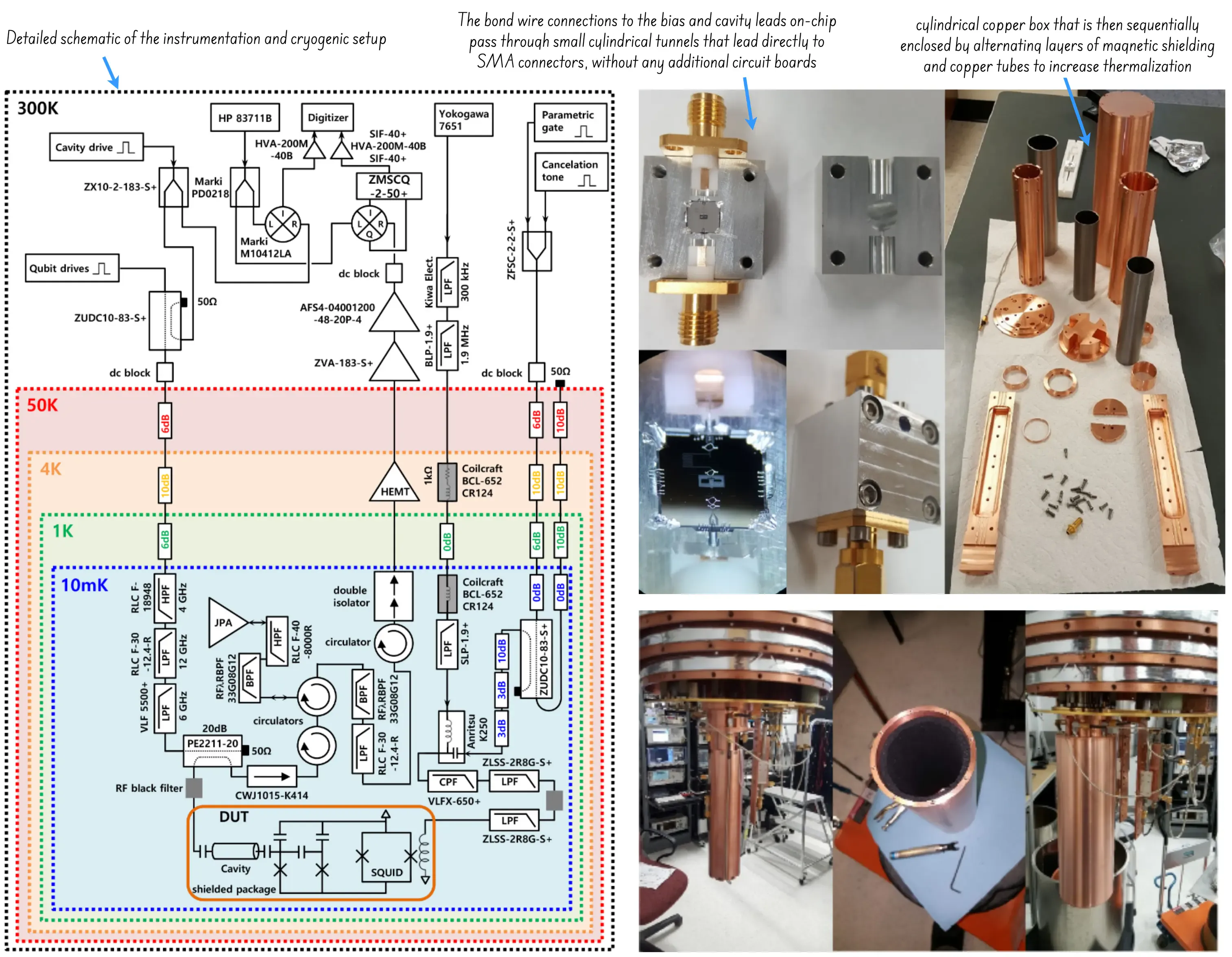 (Image source: arxiv.org/2305.02907v3)
It is worth noting that the analogy between transistors in the 60s and transmons nowadays is biased: transistors won the mainstream battle for two reasons: scalability and temperature. Silicon transistors proved incredibly easy to shrink by the billions onto a single room-temperature slice of silicon. Josephson junctions, on the other hand, require bulky, expensive cryogenic cooling systems to keep them near absolute zero.
This cryo challenge needs to be addressed for the QPU to reach scales of 10K qubits and beyond: either by using cryo pulsar to solve the cabling challenge, by using different heat-resistant modalities such as optical qubits, or by operating at higher temperature, as Spin Qubits allow for.
Conclusion Link to heading
Voilà, this short Sunday morning memo helped clarify the transmon qubit architecture. In the next “qubit modality memo series”, I will be describing the Spin Qubit Architecture.
References:
- arxiv.org/1904.06560: A Quantum Engineer’s Guide to Superconducting Qubits
- arxiv.org/2011.01261: Realization of High-Fidelity CZ and ZZ-Free iSWAP Gates with a Tunable Coupler
- arXiv.org/1812.11227v2: Analytical and numerical analysis of linear and nonlinear properties of an rf-SQUID based metasurface
- arxiv.org/2305.02907v3: Fast, tunable, high fidelity cZ-gates between superconducting qubits with parametric microwave control of ZZ-coupling
- arxiv.org/2312.13483: SQuADDS: A validated design database and simulation workflow for superconducting qubit design
- arxiv.org/2312.13483: Cryogenic Control and Readout Integrated Circuits for Solid-State Quantum Computing
- arxiv.org/1001.0816: RFSQUID-Mediated Coherent Tunable Coupling Between a Superconducting Phase Qubit and a Lumped Element Resonator
- arxiv.org/2509.04965: High-fidelity two-qubit gates with transmon qubits using bipolar flux pulses and tunable couplers
- arxiv.org/2606.03815v1: A Tutorial for Characterizing Transmon Qubits
- arxiv.org/2312.15753: Control and readout of a transmon using a compact superconducting resonator
- arxiv.org/2606.13052: Simple analytical flux-tuned iSWAP pulses for leakage suppression
- arxiv.org/2506.14128v1: Tunable Hybrid-Mode Coupler Enabling Strong Interactions between Transmons at Centimeter-Scale Distance
- springer.com/article/10.1007/s10948-025-06968-x: Implementation and Readout of Maximally Entangled Two-Qubit Gates Quantum Circuits in a Superconducting Quantum Processor
- How to make a superconducting qubit
DrawIO diagrams used in this memo: