I recently heard about Neuromorphic Processing Units, or NPUs, while discussing Neuralink.
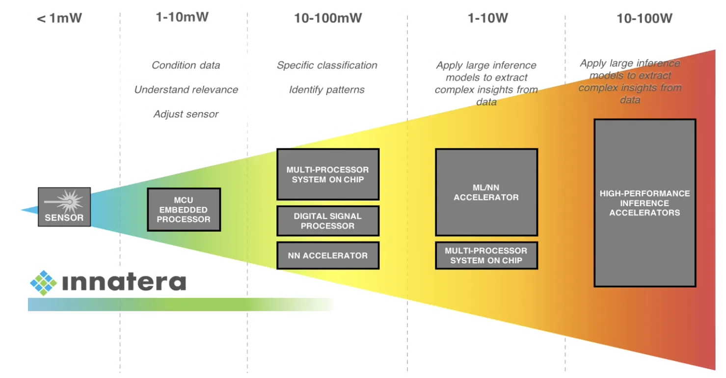
 Those NPUs have nothing to do with Quantum computing, but I thought it would be interesting to spend a bit of time getting inspired with a new processing architecture. And as a matter of fact, one of the leading IC vendors in this domain is a Dutch company called Innatera. Innatera’s latest IC, Pulsar, is based on low-power Spiking Neural Networks (see the picture on the right).
In this memo, I will try to reverse-engineer as much information as possible about how those Neuromorphic ICs are architected, how the Spiking Neural Networks are designed, and what software stack is exposed to program those devices.
Hardware Architecture Link to heading
This is an attempt to redraw the architecture diagram for the Pulsar IC (original image, complemented with insights from the white paper):
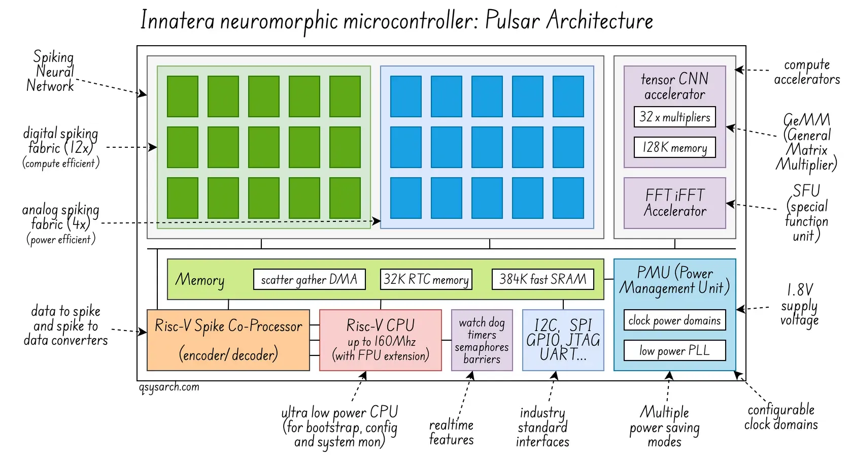
I do like the idea of using a RISC-V CPU - that’s a clear sign that the team at Innatera is making the right day-one architecture decision. In one of the diagrams from Innatera’s earlier T1 chip, the RISC-V CPU is bundled with a F extension (Floating-Point computation support).
The IC integrates many standard interfaces (SPI, I2C, …) and a power management unit (PMU) that turns on and off parts of the IC when entering “sleep mode” or “power saving” mode. Unfortunately, I could not find any data on the actual power consumption, expect from a ballpack of “less than 1mW”. Assuming a 1.8V supply voltage, this would less than 500 µA (I=W/V). I also wonder if the “per cycle” power metrics is relevant: In this case, assuming a 100Hz frequency (synaptic update period), this would mean 5 µA per synaptic update on average.
The latest diagram from Pulsar shows two accelerators: a CNN and an FFT. I believe these could be more broadly described as a GEMM (general matrix multiplier, the key for NN computation) and an SFU (special function unit, used to accelerate the FFT computation). Check the post about the GPU architecture for more information. There is also a spike encoder-decoder, which seems to have been developed as a coprocessor for RISC-V, but I could not find much more detail.
Spiking Neural Network Architecture Link to heading
The question that remains is about the Spiking Neural Network, or SNN: How does this work?
The metaphor Link to heading
I asked Gemini to give a metaphor for a 8 years old about Spiking Neural Network. Here is the story I got:
Imagine the brain like a giant post office, and the “neurons” are the little messengers who carry notes.
- Messengers and Notes:
In a normal computer program, every messenger is always talking and shouting numbers back and forth. While in a Spiking Neural Network, the messengers are very quiet and energy-efficient: They only send a quick “Hey!” message when something important happens — like a tiny electric spike.
- The Spark Meter:
Each messenger has a meter that fills up when they hear “Hey!” from others: When the meter gets full enough (reaches the threshold), that messenger gets excited too and shouts “Hey!”. Right after shouting, it resets its meter, so it can’t shout again immediately (the refractory period).
- Timing is Everything:
If a messenger hears lots of “Heys!” quickly, it means the message is super important (like “Fire!”). If a messenger shouts “Hey!” just a little bit earlier than all the others, it might be a secret sign that something special is going on (like “Tiger incoming!”). So, messengers need to be time-aware.
- Learning is the key:
The messengers learn just like you do: If Messenger A shouts “Hey!” just before Messenger B shouts “Hey!” (because something made them both excited), their friendship gets stronger, and Messenger A’s message helps Messenger B fill their meter faster next time.
SNNs are special because they are designed to be incredibly fast and efficient. They don’t waste energy talking all the time; they only activate when they have a spike of information to share! They help computers understand timing, recognize patterns, and use very little power.
The real design under the hood Link to heading
Innatera’s Thinking in Pulses blog provides a good overview of how this would be implemented in hardware. Encode the “heys” into binary values, get them through a NN, and extract the features. So far, nothing special; this is a standard NN process.

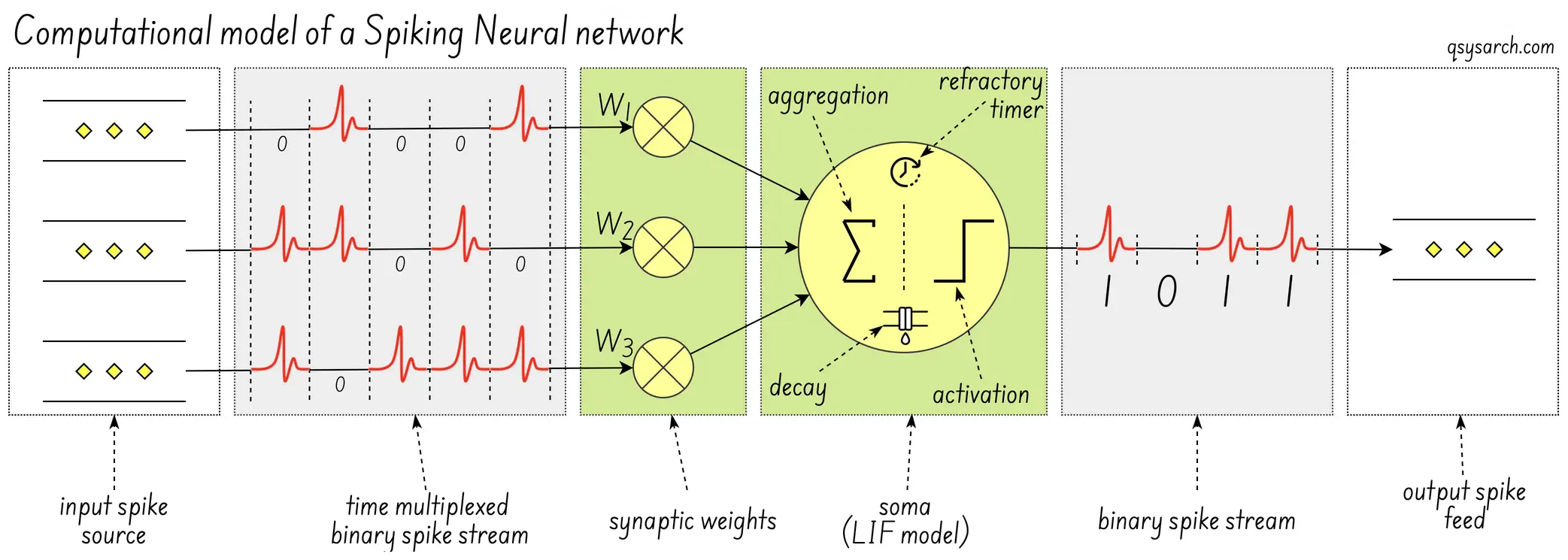
The more interesting question is how this SNN is implemented. The image below seems to be a conventional “computational model” of the digital neuron (image source) - where I have added the explicit notion of the “leaky integrate-and-fire” (LIF) within the SOMA.
What makes the hardware implementation low-power Link to heading
to be completed: explanations needed for
the performance gain (10x, 1000x, or more?)
the achievable NN propagation latencies
the tradeoffs and limitations
analog vs digial design performance.
power consumption relative to GPUs/TPUs
Innatera’s core design Link to heading
One question from the Pulsar design is: why are there two SNNs? The answer is that Innatera’s analog (proprietary analog-mixed signal) SNN fabric is optimized for maximum energy efficiency and very fast, ultra-low-power event processing. While the digital SNN fabric is a more programmable and flexible design that supports more configurable networks at slightly higher power. (Source)
There is not much information on Innatera’s website about the inner architecture of their spiking neural network, but fortunately, they have a few patents we can try to reverse-engineer!
| Filing Date | Publication Number | Title (Abbreviated) |
| 2021-02-09 | US20220230051A1 | Spiking Neural Network |
| 2021-12-09 | EP4505212A1 | Method for efficient radar pre-processing |
| 2022-01-26 | EP4323923B1 | Hierarchical reconfigurable multi-segment spiking neural network |
| 2022-02-14 | EP4238006A2 | Distributed multi-component synaptic computational structure |
| 2022-03-22 | EP4226281B8 | Adaptation of snns through transient synchrony |
| 2022-04-08 | EP4548260A1 | Calibration of spiking neural networks |
| 2022-06-03 | EP4562540A | System and method for efficient feature-centric analog to spike encoders |
| 2022-06-24 | EP4573485A1 | Sequential neural machine for memory optimized inference |
| 2022-09-08 | WO2024038102A1 | System and method for reconfigurable modular neurosynaptic computational … |
| 2022-10-18 | WO2024153705A1 | Self-timed feedforward synthesizable and technology scalable mixed-signal … |
| 2023-05-18 | WO2024175770A1 | Always-on neuromorphic audio processing modules and methods |
| 2023-05-24 | WO2024175767A1 | System and method for mapping of spiking neural networks on neuromorphic … |
| 2023-06-19 | WO2025012331A1 | Method for training machine learning models for stochastic substrates |
| 2023-06-22 | WO2025017094A1 | Method to build and deploy spiking neural networks on hardware device |
| 2023-10-23 | WO2025021573A1 | System and method for occupancy detection using a frame-based sensor |
| 2023-12-06 | WO2025062034A1 | Feature extraction and encoding of spiking neural networks using convolutional |
| 2024-03-08 | WO2023242374A1 | Spike interconnect on chip single-packet multicast |
This is quite a lot of patents for a startup! For the sake of time, I have only been looking at the first and last patent in this list.
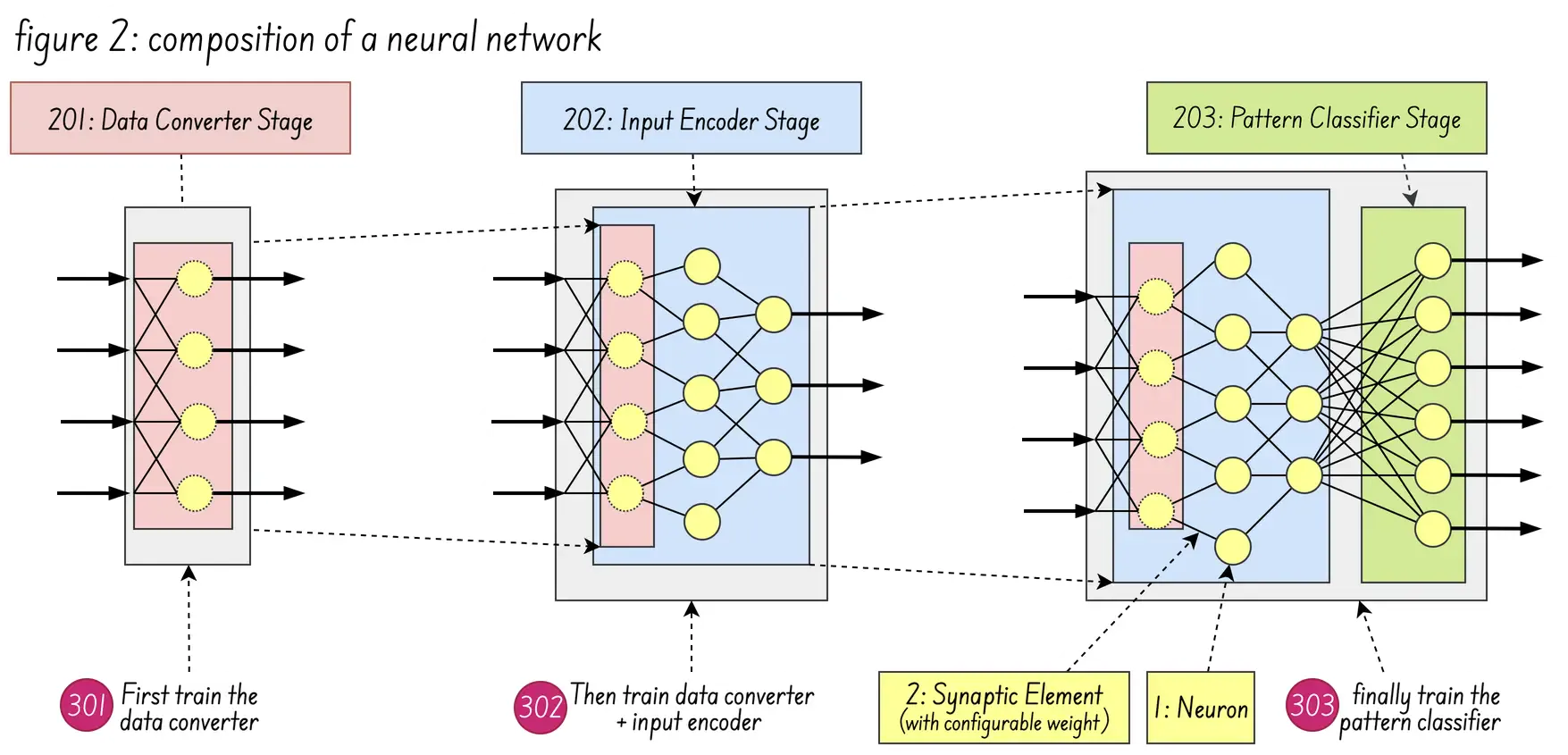
Let’s start with the first patent US20220230051A1, which seems to be the closest one to describe the actual HW implementation of the SNN: The patent is centered on a compositional methodology for building SNNs from specialized, pre-trained sub-networks (“cells”) using a “unique response” principle.
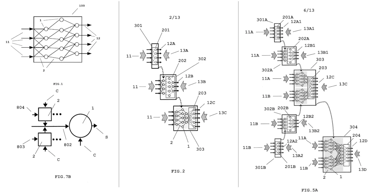
Figure 2 (below) shows the composition of a neural network formed by the integration of a data converter stage 201, input encoder stage 202, and pattern classifier stage 203. As for figure 5B (above) it shows how multiple temporal spike trains are fused into a single fused spike train
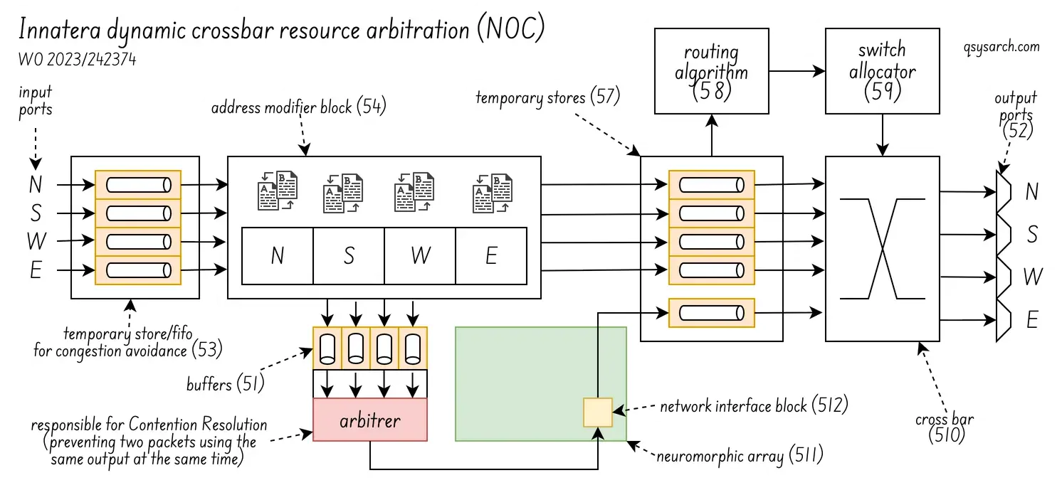
As for the last patent WO2023242374A1, it discloses Innatera’s Spiking Neural Network architecture, used to efficiently implement single-packet multicast using network-on-chip networks. The goal is to reduce duplication, latency, and overhead in multicore/many-core systems for multicast communication.
The diagram below (figure 5 in the patent) shows how the NOC arbitration works. The idea is to prevent two spikes (or more) having to be sent to the same output port at the same time. This is an efficient way to route spikes each cycle. Although, I wonder how deep are the fifos in the actual hardware.

What is not clear to me is how the core and the spike network fit together: How many neurons are in a core? Are the core interconnected or working together? Or are they independant units that can process independent classification in parallel?
Other Neural Core Design Link to heading
I do not have the answer about the exact Innera’s core architecutre, but there are a lot of research papers giving more details about the possible implementations. The paper “a system design perspective on neuromorphic computer processors ” is particularily interresting since it compares serveral architectures.
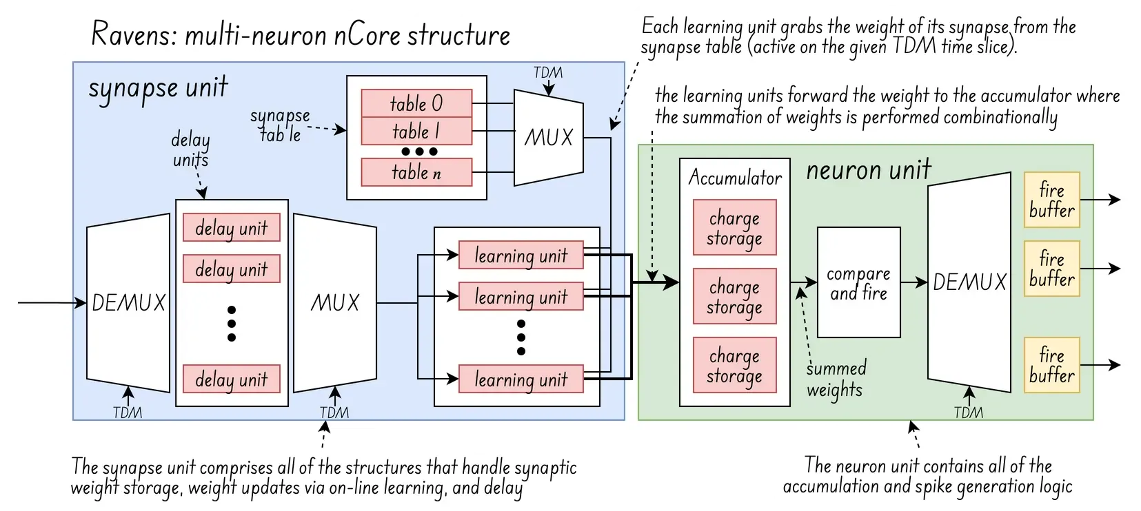
One of those architectures is the “reconfigurable and very efficient neuromorphic system”, or RAVENS, which is shown in the diagram below:
 (diagram updated from the original image: )
The idea behind RAVENS is to pipeline several “virtual neurons” using time-division multiplexing (TDM), in a two stage process consisting of accumulation and update.
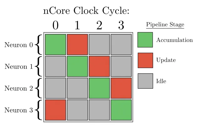
accumulation stage: a neuron accumulates charge from the input synapses connected to it and determines whether a fire event should occur or not based on its programmed threshold and refractory status
update stage: include on-line learning changes to synaptic weights, leaking charge , increments to refractory counters, accumulated charge changes due to transitioning out of a refractory period
The interresing part here is the on-line learning: In neuromorphic ICs, online learning changes synaptic weights by using algorithms like Hebbian learning or reinforcement learning to adjust synaptic strength in real-time based on input from pre- and post-synaptic neurons.
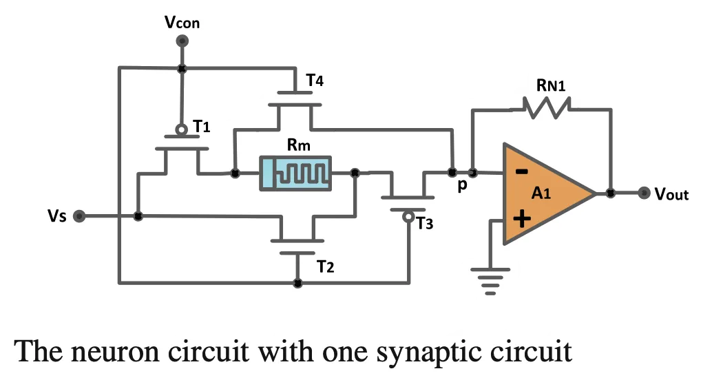
In the case of analog cores, this adjustment is physically implemented through devices like memristors or magnetic tunnel junctions (MTJs), whose resistance or conductance state is modulated by neural activity, directly representing and storing the synaptic weights. And in the case of digital cores, it is done via the synpase tables, at least of RAVENS.
Software Stack: TALAMO Link to heading
High-level stack Link to heading
Innatera’s offering includes a bundled Talamo SDK, which doesn’t require SNN expertise, supports end-to-end applications, and uses a standard deep learning workflow. The Talamo kit helps developers build spiking models from scratch in a PyTorch-based environment. It’s a battery included.
The compilation workflow is very standard. The diagram below is a slightly updated version of Innatera’s original material, assuming the brain part of the workflow is the compiler. I also wonder if the simulator is taking the binary executable as input, in which case it would be called an emulator. One thing that would be very good to get more information about is the optimzation process, and whether there are parameters that can be tweeked by the user (like reducing the weights to 1.58 bits).

Once the binary program has been generated, this execution workflow is used, and follows more or less the process defined in the patent WO2023242374A1.

Low-level stack Link to heading
Innatera’s hardware includes a powerful RISC-V, a capable GEM, and an SFU compute accelerator. Some power users might find this more appealing to have a bare metal access to this hardware, compared to just loading weights into a C library targetable for Innatera’s architecture.
Maybe offering some form of open-source firmware SDK would be beneficial. Alternatively, one could think of CudaNN, exposing a General Purpose Neural Processor Unit (GPNPU) experience, just like Cuda-Q exists for the Quantum industry. As well as an NVNLink, similar to NVQLink, enabling large scale NPU networks and hybrid architectures?
Maybe this is what is meant in the road to commercial success for neuromorphic technologies : “it was not until the advent of simple programming models and tools, simultaneous with straightforward API access to hardware, that tensor processors reached widespread adoption”. Just replace tensor processors with neuromorphic processing units (NPU)?
To me, this boils down to user experience (UX) and developper experience (DX). And I am firm believer that ease of use and developer experience are among the key-enablers, or strategy pillars, in creating genuinely outstanding product experiences.
 (Image credits: archi monarch)
Conclusion Link to heading
That wraps up this quick memo on the high-level architecture of Neuromorphic ICs. Without a doubt, this hardware architecture is an alternative, powerful technology with significant potential. Yet, one could argue that Neuromorphic ICs lack a killer application. But isn’t it the exciting part about Neuromorphic ICs? Does that mean the world that goes with it has to be created?
I do believe that the team at Innetera is among “the people who see the world differently”. And amid concerns about AI data centers’ voracious appetite for watts, aren’t neuromorphic ICs one answer to the essential question: How to get more value out of less energy? If this is the case, then what will it take to scale the Neuromorphic ICs to reach the level of compution power equivalent to what is needed by the AI data centers?
Also, I wonder if adding a bit of sillicon photonics to the SNN would be of any help? It could either for the sake of neural computation, but also for the sake of creating a large scale interconnecting network between the SNN ICs.
References Link to heading
- A Multi-Context Neural Core Design for Reconfigurable Neuromorphic Arrays
- Low-latency hierarchical routing of reconfigurable neuromorphic systems
- Mosaic: in-memory computing and routing for small-world spike-based neuromorphic systems
- Neuromorphic Computing in the Netherlands
- Neuromorphic Computing: Energy-efficient smart chip design
- Development of a Neuromorphic Computing System
- TrueNorth: A Deep Dive Into IBM’s Neuromorphic Chip Design
- The road to commercial success for neuromorphic technologies
- A system design perspective on neuromorphic computer processors
- Rapidly develop and deploy next-generation neuromorphic AI
- Integrated platforms and techniques for photonic neural networks
- Photonic Spiking Neural Networks
- Matrix Core Programming on AMD architecture
DrawIO diagrams used in this memo:
