Source: A Cryogenic Interface for Controlling Many Qubits (arXiv:1912.01299)
There are several kinds of qubit modalities, and one of the promising ones is the superconducting qubit.
The challenge with the superconducting qubit modality is that it is highly sensitive to environmental noise and has shorter lifespans than other modalities. Additionally, superconducting qubits require operation at cryogenic temperatures, necessitating the use of specialized cooling systems.
The objective of the cryogenic system is to reach near absolute zero (< 0.1 K), thereby minimizing interference from thermal energy. Qubits are sensitive entities, so the less the interference, the better.
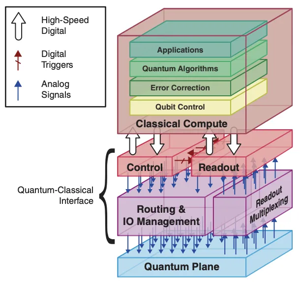
Cryogenic Quantum QPU Link to heading
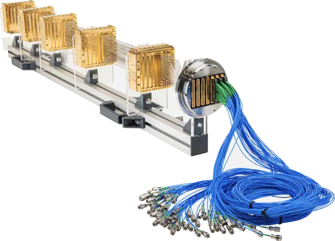
There are several aspects to consider regarding cryo: first, having the QPU located in the fridge, while the control stack operates at room temperature. This is already possible today with solutions from Bluefors - but that creates the so-called “wiring bottleneck” at the interconnecti*on level.
Fortunately, the industry is very proactive in addressing this challenge, and many high-density wiring solutions are available, and even integrated with the fridge (see picture on the right).
Cryogenic Digital to Analog Converters (DAC) Link to heading
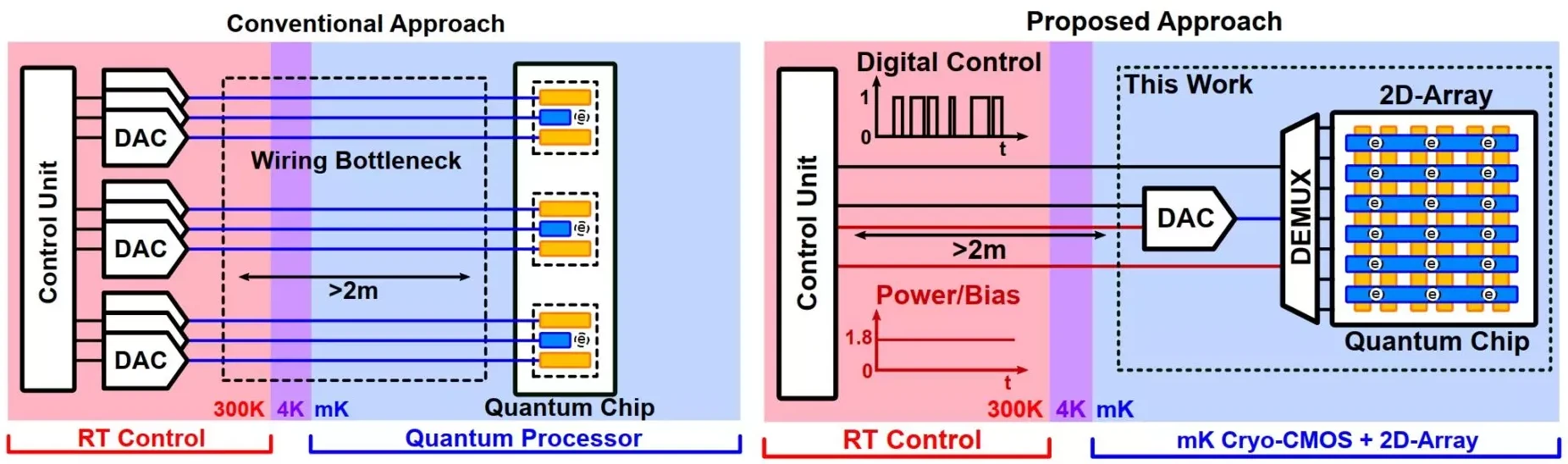
The second aspect is to operate the control stack at a much lower temperature. The interesting aspect of operating at lower temperatures is that the noise level must be kept to a minimum to prevent qubit interference. So, Cryo-CMOS is emerging as a key enabling technology for large-scale quantum computers and other applications constrained by the wiring bottleneck.
In the diagram below from TU Deflt, sensitive analog signals are indicated in blue, while the more robust digital and supply/bias lines are in black and red, respectively. The principal objective is to minimize the signals in blue.
Cryogenic Control Asics Link to heading
One of the many challenges that come with cryo-ASICs is that the Physical behavior of CMOS technology at cryogenic temperatures, including power dissipation and thermal budget, must be kept low. And so, the third aspect is to have full control of the ASIC to operate at cryogenic temperatures.
For example, on the diagram below, the FPGA is now located at 4K (-269,15 °C), and knowing how much the FPGA is heating, this becomes a huge challenge compared to only having the DAC at 4K (Which in itself is also a huge challenge!).
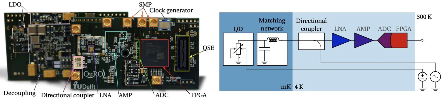 (Source: Cryogenic electronics for the read-out of quantum processors)
Case Study: Google: On the Path to Cryogenic Control of Quantum Processors Link to heading
Although the paper and video from Google are already quite old (2019), it is full of very relevant information.
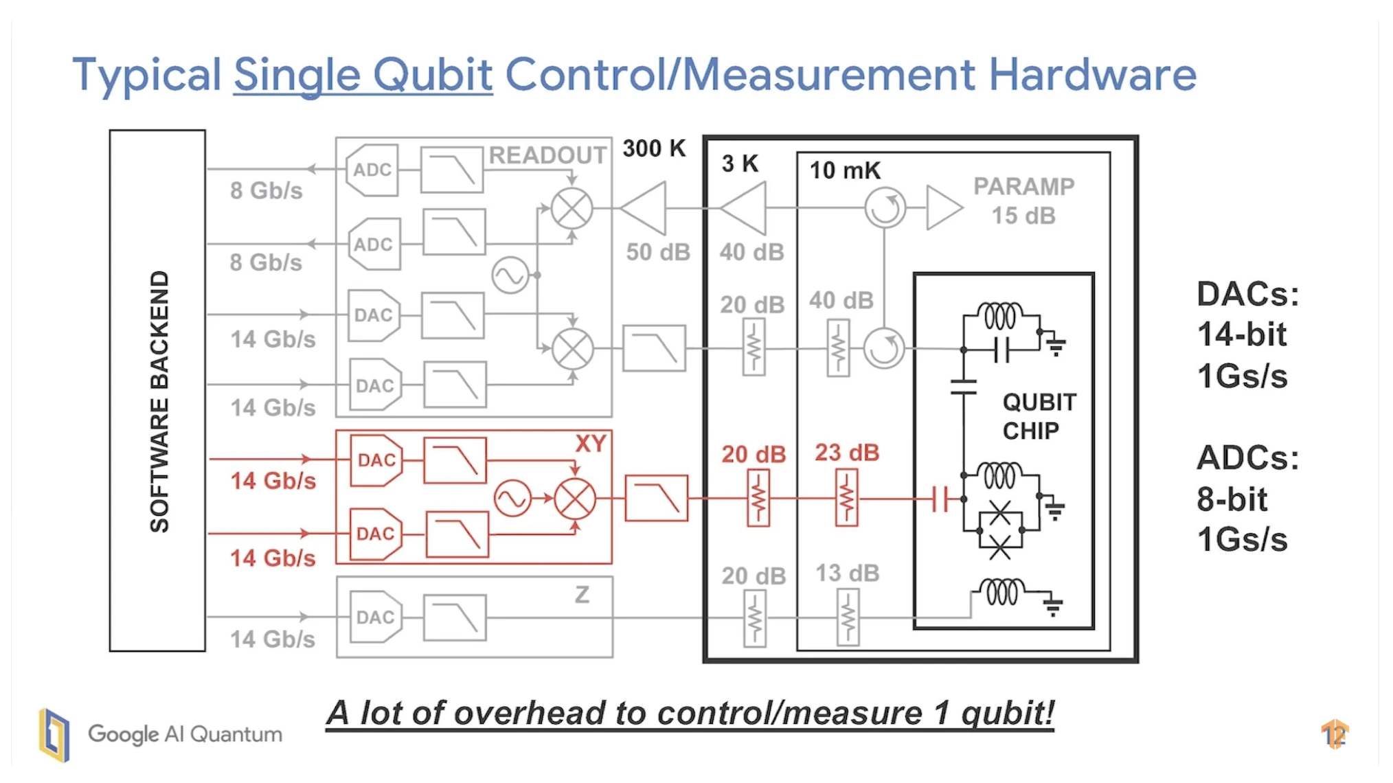
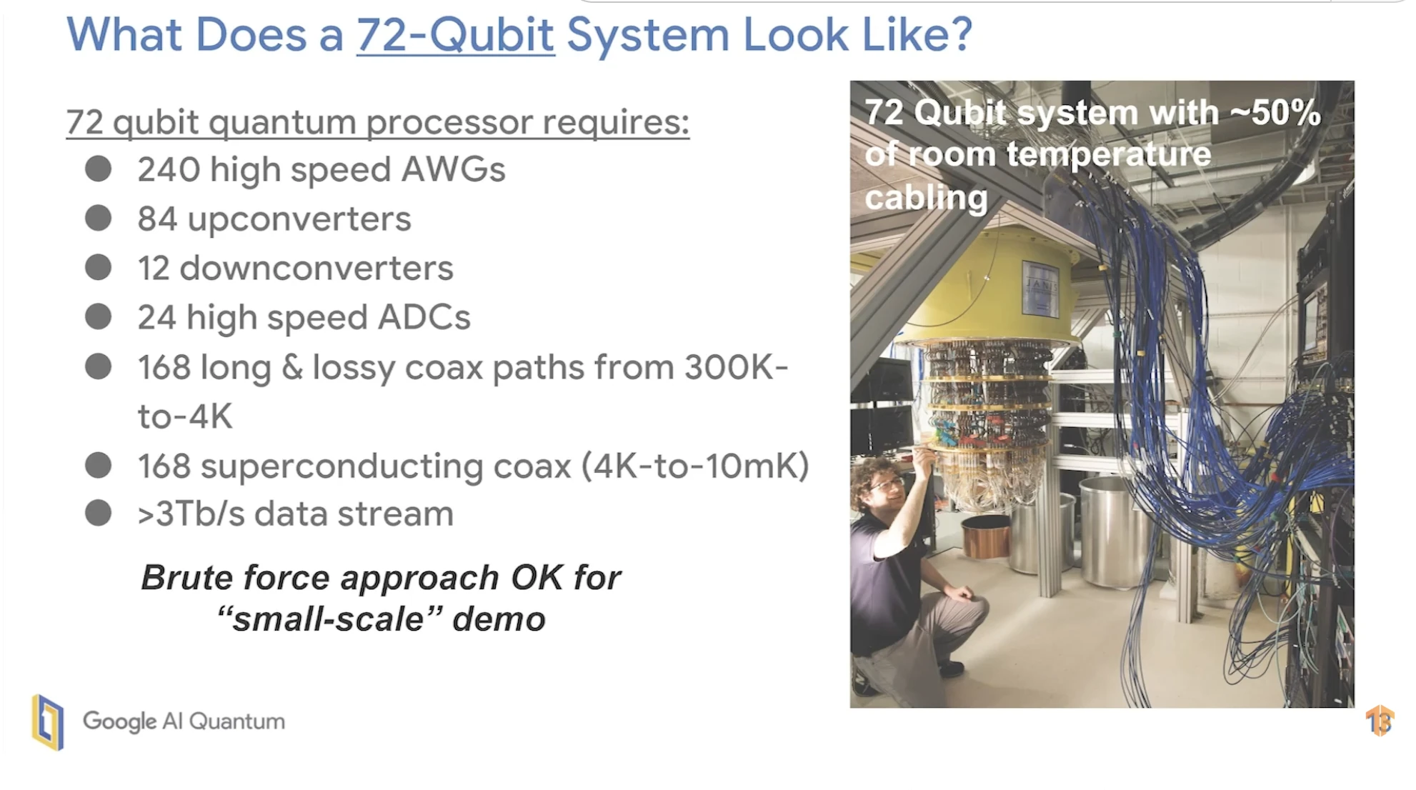
The issue with the current “Single Qubit” control and measurement hardware, when scaled with the temperature staging distribution (i.e., with readout at 300K or ~25°C), is the cabling bottleneck. The picture on the right shows how many cables are needed when scaling the system to a 72-qubit system, together with a useful approximation of the number “components” per qubit (where components refers to the DAC,ADC,AWG,etc)
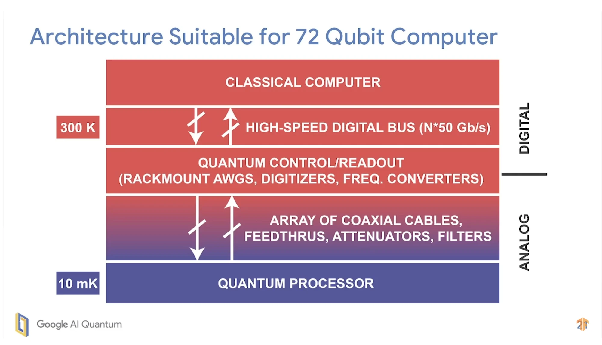
Those two next slides show the proposed split from the Google team on the “cryo-staging”, which, without any surprises, fits with the previous concepts of moving the control to 4K. The interesting part is that, for Google, the Digital domain is split into two parts, operating at both 4K and 300K.
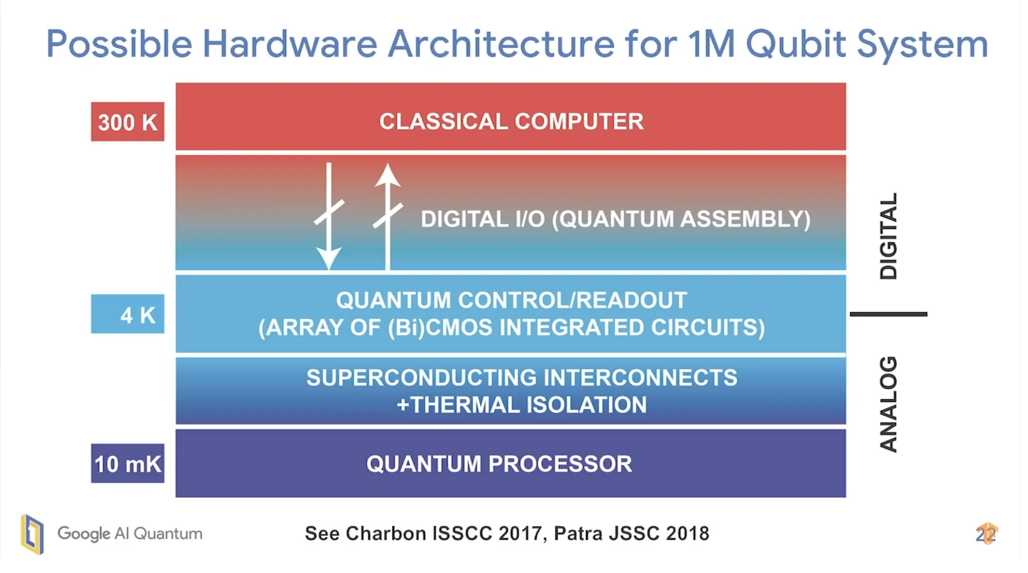
Looking into the details of the 4K parts of the digital control, Google came up with a very simple yet clever approach to the AWG (pictured on the left). The interconnection to the 300K control domain is materialized in the form of a memory for storing the AWG samples.
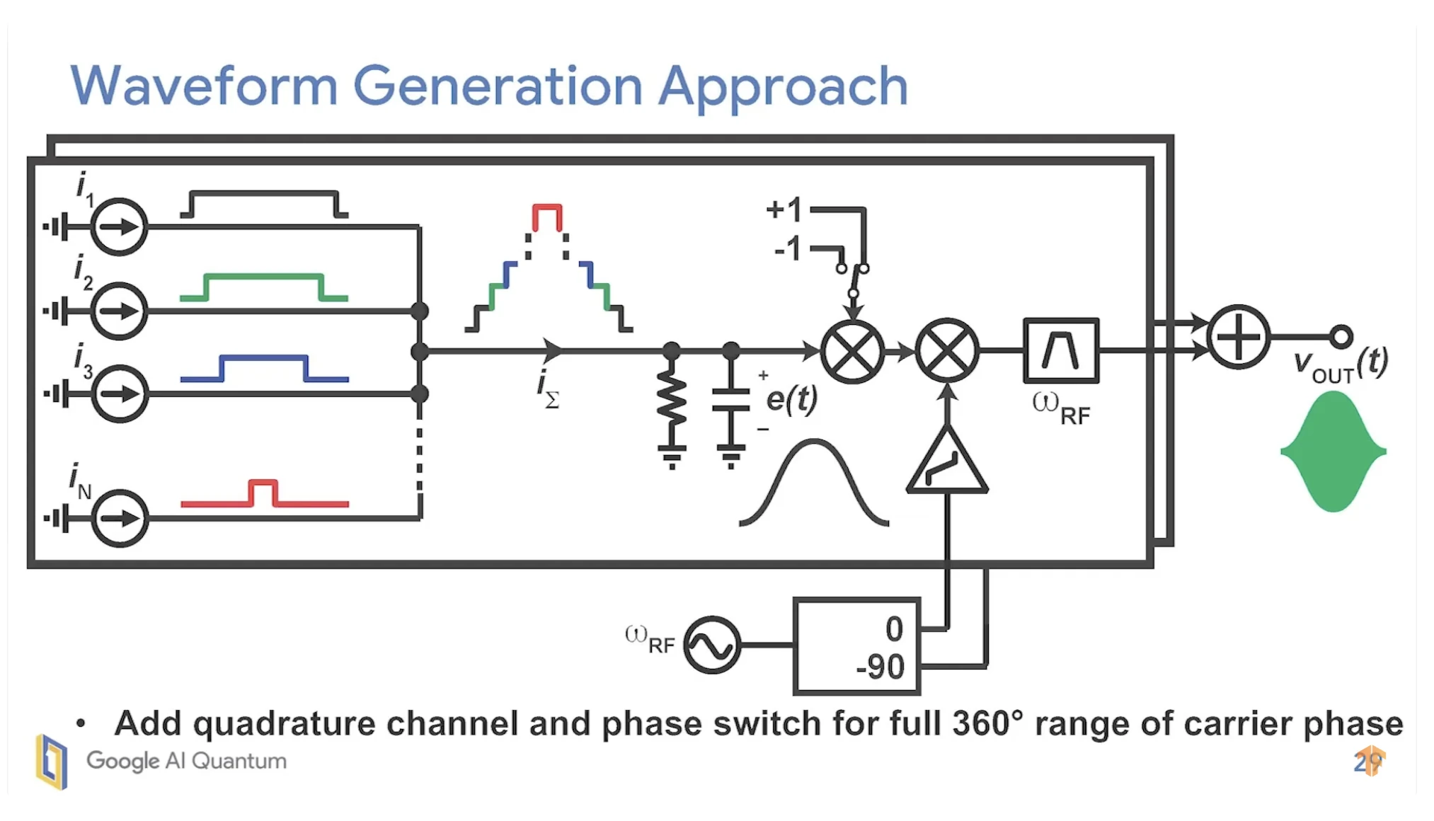
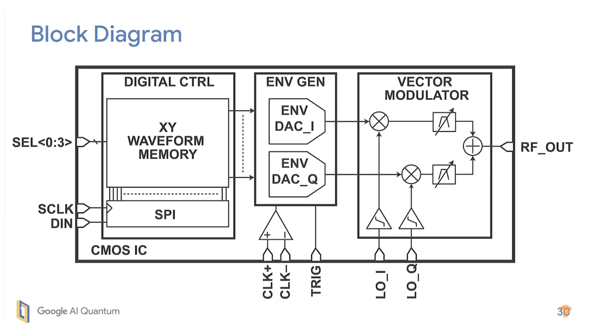
What I do like in the above proposal is that the computation logic, or classical computation (CC), remains at 300K, and the interface between the computation logic and the real-time signal generation is implemented using memory. This memory needs to be small, and that’s why there should be a tight coupling between the CC and the AWG. Unfortunately, there is limited public information available about this interface.
Conclusion Link to heading
Without a doubt, the industry will be able to produce cryogenic ASIs within 5 to 10 years, with a complete digital front-end comprising voltage regulators, clock generation, and a reconfigurable digital core that operates at deep-cryogenic temperatures. This will help overcome the “cabling bottleneck”.
On the other hand, other modalities, such as optically addressable qubits, which can be operated at room temperature, may experience a breakthrough that will bring them on par with silicon qubits.
Either way, one can assume that this challenge will be overcome within a decade.
Voilà, this Sunday morning memo did not delve into any sort of detail, but laid the groundwork for understanding the reasons, challenges, and solutions for operating quantum entities (the qubits) at cryogenic temperatures.
Resources and further readings Link to heading
- Cryogenic Front-End ASICs for Low-Noise Readout of Charge Signals
- A System-on-Chip (SoC) for Charge Readout in the nEXO Experiment
- Cryogenic electronics for the read-out of quantum processors
- A Cryogenic Interface for Controlling Many Qubits
- Control of transmon qubits using a cryogenic CMOS integrated circuit
Chat GPT reverse-prompting on the difference between a computer and a machine.

(prompts: ‘Can you draw a cartoon image of a “cryogenic quantum computer”’ vs ‘Can you draw a cartoon image of a “cryogenic quantum machine’)